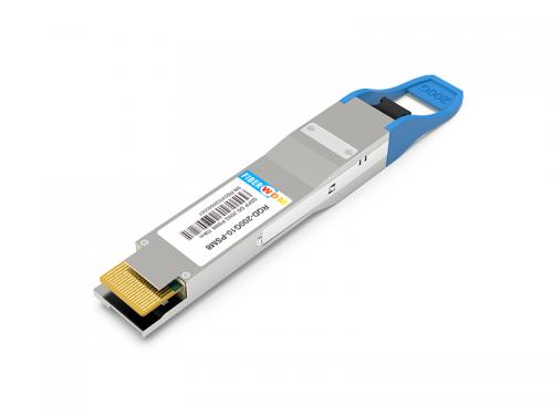

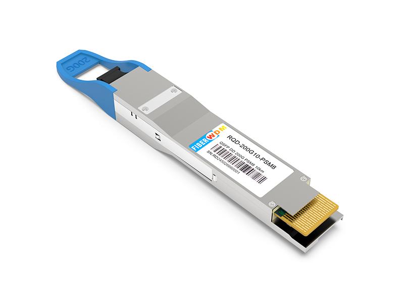
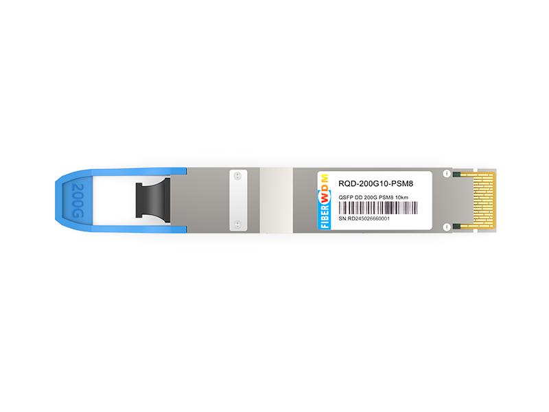
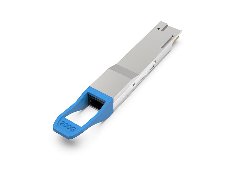
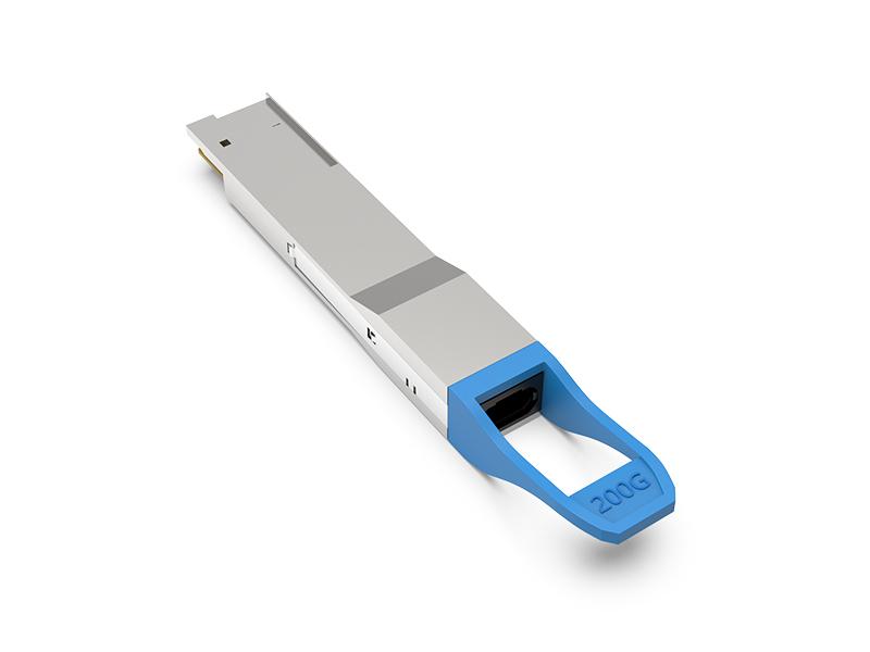
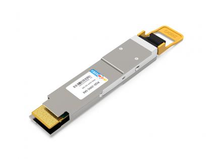
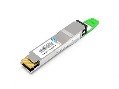
The FiberWDM RQD-200G10-PSM8 is a Eight-Channel, Pluggable, Parallel, Fiber-Optic QSFP DD PSM8 for 2×100 Gigabit Ethernet , Infiniband DDR/EDR Applications. This transceiver is a high performance module for data communication and interconnect applications. It integrates eight data lanes in each direction with 208 Gbps bandwidth. Each lane can operate at 26Gbps up to 10km over G.652 SMF. These modules are designed to operate over singlemode fiber systems using a nominal wavelength of 1310nm. The electrical interface uses a 76 contact edge type connector. The optical interface uses an 24 fiber MTP (MPO) connector. This module incorporates FiberWDM proven circuit and Optical technology to provide reliable long life, high performance, and consistent service.
200Gb/s QSFP DD PSM8 10km Optical Transceiver RQD-200G10-PSM8
Features
Applications

Figure 1. Module Block Diagram
The 200Gb/s QSFP DD PSM8 is one kind of parallel transceiver. DFB and PIN array package is key technique, through I2C system can contact with module.
Absolute Maximum Ratings
| Parameter | Symbol | Min | Min | Unit |
| Supply Voltage | Vcc | -0.3 | 3.6 | V |
| Input Voltage | Vin | -0.3 | Vcc+0.3 | V |
| Storage Temperature | Ts | -20 | 85 | ºC |
| Case Operating Temperature | Tc | 0 | 70 | ºC |
| Humidity (non-condensing) | Rh | 5 | 95 | % |
Recommended Operating Conditions
| Parameter | Symbol | Min | Typical | Max | Unit |
| Supply Voltage | Vcc | 3.13 | 3.3 | 3.47 | V |
| Operating Case Temperature | Tc | 0 | 70 | ºC | |
| Data Rate Per Lane | fd | 10.3125 | 25.78125 | Gbps | |
| Humidity | Rh | 5 | 85 | % | |
| Power Dissipation | Pm | 5.28 | 6.5 | W | |
| Fiber Bend Radius | Rb | 0.002 | 10 | km |
Electrical Specifications
| Parameter | Symbol | Min | Typical | Max | Unit |
| Differential Input Impedance | Zin | 90 | 100 | 110 | ohm |
| Differential Output Impedance | Zout | 90 | 100 | 110 | ohm |
| Differential Input Voltage Amplitude1 | ΔVin | 190 | 700 | mVp-p | |
| Differential Output Voltage Amplitude2 | ΔVout | 300 | 850 | mVp-p | |
| Input Logic Level High | VIH | 2.0 | Vcc | V | |
| Input Logic Level Low | VIL | 0 | 0.8 | V | |
| Output Logic Level High | VOH | Vcc-0.5 | Vcc | V | |
| Output Logic Level Low | VOL | 0 | 0.4 | V |
Note:
1. Differential input voltage amplitude is measured between TxnP and TxnN.
2. Differential output voltage amplitude is measured between RxnP and RxnN.
Optical Characteristics
| Parameter | Symbol | Min | Typical | Max | Unit |
| Transmitter | |||||
| Centre Wavelength | λc | 1295 | 1310 | 1325 | nm |
|
Side-mode suppression ratio |
SMSR | 30 | dB | ||
| Average Launch Power (each lane) | PAVG | -4 | 2 | dBm | |
|
Optical Modulation Amplitude (each lane) |
POMA | -5.0 | 2.2 | dBm | |
| TDP,each lane | TDP | 2.9 | dB | ||
|
Extinction Ratio |
ER | 3.5 | dB | ||
|
Relative Intensity Noise |
RIN | -128 | dB/Hz | ||
|
Optical Return Loss Tolerance |
TOL | 20 | dB | ||
|
Transmitter Reflectance |
RT | -12 | dB | ||
|
Average Launch Power of OFF Transmitter (each lane) |
POFF | -30 | dB | ||
|
Eye Mask Coordinates1: X1, X2, X3, Y1, Y2, Y3 |
{0.31,0.4,0.45,0.34,0.38.0.4} Hit Ratio = 5x10⁻⁵ |
||||
|
Receiver |
|||||
|
Center Wavelength |
λc | 1295 | 1310 | 1325 | nm |
|
Damage Threshold,each lane |
THd | 3.0 | dBm | ||
|
Average Receive Power, each lane |
-12.66 | 2.0 | dBm | ||
|
Receive power, each lane (OMA) (max) |
2.2 | dBm | |||
|
Receiver Reflectance |
RR | -26 | dBm | ||
|
Receiver Sensitivity (OMA), each lane |
SEN | -9.5 | dBm | ||
|
LOS Assert |
LOSA | -18 | dBm | ||
|
LOS De-Assert – OMA |
LOSD | -16 | dBm | ||
|
LOS Hysteresis |
LOSH | 0.5 | 3 | dB | |
Note:
1. Even if the TDP<1dB,the OMA min must exceed the minimum value specified here.
2. The receiver shall be able to tolerate, without damage, continuous exposure to a modulated optical input signal having this power level on one lane. The receiver does not have to operate correctly at this input power.
3. Sensitivity is specified at 1E-12 BER at 25.78125Gb/s.
Pin Description


Figure 2. Electrical Pin-out Details
ModSelL Pin
The ModSelL is an input signal that must be pulled to Vcc in the QSFP-DD module. When held low by the host, the module responds to 2-wire serial communication commands. The ModSelL allows the use of multiple QSFP-DD modules on a single 2-wire interface bus. When ModSelL is “High”, the module shall not respond to or acknowledge any 2-wire interface communication from the host.
In order to avoid conflicts, the host system shall not attempt 2-wire interface communications within the ModSelL de-assert time after any QSFP-DD modules are deselected. Similarly, the host must wait at least for the period of the ModSelL assert time before communicating with the newly selected module. The assertion and de-asserting periods of different modules may overlap as long as the above timing requirements are met.
ResetL Pin
The ResetL signal shall be pulled to Vcc in the module. A low level on the ResetL signal for longer than the minimum pulse length (t_Reset_init) (See Table 13 ) initiates a complete module reset, returning all user module settings to their default state.
InitMode Pin
InitMode is an input signal. The InitMode signal must be pulled up to Vcc in the QSFP-DD module. The InitMode signal allows the host to define whether the QSFP-DD module will initialize under host software control (InitMode asserted High) or module hardware control (InitMode deasserted Low). Under host software control, the module shall remain in Low Power Mode until software enables the transition to High Power Mode, as defined in Section 7.5. Under hardware control (InitMode de-asserted Low), the module may immediately transition to High Power Mode after the management interface is initialized. The host shall not change the state of this signal while the module is present. In legacy QSFP applications, this signal is named LPMode. See SFF-8679 for signal description.
ModPrsL Pin
ModPrsL must be pulled up to Vcc Host on the host board and grounded in the module. The ModPrsL is asserted “Low” when the module is inserted and deasserted “High” when the module is physically absent from the host connector.
IntL Pin
IntL is an output signal. The IntL signal is an open collector output and must be pulled to Vcc Host on the host board. When the IntL signal is asserted Low it indicates a change in module state, a possible module operational fault or a status critical to the host system. The host identifies the source of the interrupt using the 2-wire serial interface. The IntL signal is deasserted “High” after all set interrupt flags are read.
Power Supply Filtering
The host board should use the power supply filtering shown in Figure 3.

Figure 3. Host Board Power Supply Filtering
Optical Interface Lanes and Assignment
The optical interface port is a male MPO24 connector .

Figure 4. Optical Receptacle and Channel Orientation
DIAGNOSTIC MONITORING INTERFACE
Digital diagnostics monitoring function is available on all FiberWDM QSFP DD products. A 2-wire serial interface provides user to contact with module.
The structure of the memory is shown in Figure 5. The memory space is arranged into a lower, single page, address space of 128 bytes and multiple upper address space pages. This structure permits timely access to addresses in the lower page, e.g. Interrupt Flags and Monitors. Less time critical entries, e.g. serial ID information and threshold settings, are available with the Page Select function. The structure also provides address expansion by adding additional upper pages as needed.
The interface address used is A0xh and is mainly used for time critical data like interrupt handling in order to enable a one-time-read for all data related to an interrupt situation. After an interrupt, IntL, has been asserted, the host can read out the flag field to determine the affected channel and type of flag.

Figure 5. QSFP28 Memory Map

Figure 6. Low Memory Map


Figure 7. Page 00 Memory Map
Timing for Soft Control and Status Functions

Figure8. Timing Specifications
Mechanical Dimensions

Figure10. Mechanical Specifications
Regulatory Compliance
RQD-200G10-PSM8 are Class 1 Laser Products. They are certified per the following standards:
| Feature | Agency | Standard |
| Laser Eye Safety | FDA/CDRH | CDRH 21 CFR 1040 and Laser Notice 50 |
| EMC | FCC | 47 CFR FCC Part 15 Subpart B |
| EMC | CE-EMC |
EN 55032:2015 EN55035:2017 |
Complies with FDA performance standards for laser products except for deviations pursuant to Laser Notice No. 50, dated June 24, 2007.
References
1. QSFP DD MAS Rev4.0
2. Ethernet 100GBASE-PSM4 IEEE802.3bm
CAUTION:
Use of controls or adjustment or performance of procedures other than those specified herein may result in hazardous radiation exposure.
Ordering Information
| Part Number | Product Description |
| RQD-200G10-PSM8 | QSFP DD, 2x100GBASE-PSM4, MPO Connector, reach 10km on G.652 |
Important Notice
Performance figures,data and any illustrative material provided in this data sheet are typical and must be specifically confirmed in writing by FiberWDM before they become applicable to any particular order or contract. In accordance with the FiberWDM policy of continuous improvement specifications may change without notice.
The publication of information in this data sheet does not imply freedom from patent or other protective rights of FiberWDM or others. Further details are available from any FiberWDM sales representative.
Want to know about this product?
If you are interested in our products and want to know more details,please leave a message here,we will reply you as soon as we can.
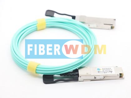
 200G QSFP56 FR4 2KM LC PAM4 Optical Transceiver
 200G QSFP56 SR4 100m 850nm PAM4 Transceiver
 200G QSFP-DD SR8 100m Optical Transceiver
 QSFPDD 200G 2xCWDM4 2km Optical Transceiver
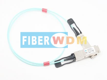
 QSFPDD 200G PSM8 10km Optical Transceiver (MPO16)
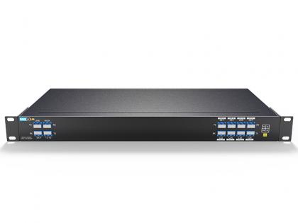
 Splitter PLC 2X64 LC/APC 1U Rack 440*200*44mm
 1650nm Reflector LC/APC
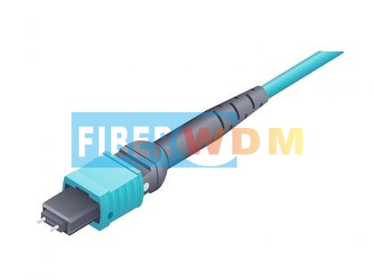
 4 Channels MPO TO Dual LC Device 2U Rack

Address : Room 901, Building 6, JD Smart Industrial Park, No. 128, Juhua Stone Avenue, Huashan Town, Huadu District, Guangzhou City
Tel : +86 15989256178
Whatsapp : +86 15914235380
Email : sales@fiberwdm.com