
The 1600G OSFP1600 2xDR4 Transceiver is designed to transmit and receive serial optical data links up to 212.5 Gbps data rate (per channel) by PAM4 modulation format over single-mode fiber. It is a small-form-factor hot pluggable transceiver module integrated with high performance Sipho modulator. It is compliant with 1600G Ethernet specs and OSFP MSA.
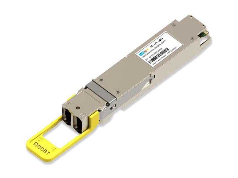
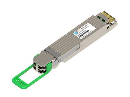
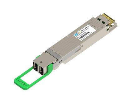
1600G OSFP1600 2xDR4 500M 1.6T Optical Transceiver
RO-1T6-2DR4
The 1600G OSFP1600 2xDR4 Transceiver is designed to transmit and receive serial optical data links up to 212.5 Gbps data rate (per channel) by PAM4 modulation format over single-mode fiber. It is a small-form-factor hot pluggable transceiver module integrated with high performance Sipho modulator. It is compliant with 1600G Ethernet specs and OSFP MSA.
Features
|
Applications
|
Standards
|
Specifications
(Tested under recommended operating conditions, unless otherwise noted)
|
Parameter |
Min |
Typ |
Max |
Unit |
Notes |
|
Transmit characteristics |
|||||
|
Signaling rate |
106.25 -50ppm |
106.25 |
106.25 +50ppm |
GBd |
|
|
Modulation format |
PAM4 |
||||
|
Wavelength |
1304.5 |
1311 |
1317.5 |
nm |
|
|
Side-mode suppression ratio(SMSR) |
30 |
dB | |||
|
Average launch power |
-3.3a |
4 |
dBm |
||
|
Outer Optical Modulation Amplitude(OMAouter) |
4.2 |
dBm |
|||
|
Outer Optical Modulation Amplitude (OMAouter) |
|||||
|
for TDECQ < 0.9 dB |
-0.3 |
dBm |
|||
|
for 0.9 dB ≤max(TECQ,TDECQ) ≤ 3.4 dB |
-1.2 + max(TECQ,TDECQ) |
dBm |
|||
|
Transmitter and dispersion eye closure for PAM4(TDECQ) |
3.4 | dB | |||
|
Extinction ratio |
3.5 |
dB |
|||
|
Transmitter transition time |
8 |
ps |
|||
|
Average launch power of OFF transmitter |
-15 |
dBm |
|||
|
RIN21.4OMA |
-139 |
dB/Hz |
|||
|
Optical return loss tolerance |
21.4 |
dB |
|||
|
Transmitter reflectance |
-26 |
dB |
|||
|
Receive characteristics |
|||||
|
Signaling rate |
106.25 -50ppm |
106.25 |
106.25 +50ppmc |
GBd |
|
|
Modulation format |
PAM4 |
|
|||
|
Wavelength |
1304.5 |
1311 |
1317.5 |
nm |
|
|
Damage threshold |
5 |
dBm |
|||
|
Average receive power |
-5.8d |
4 |
dBm |
||
|
Receive power (OMAouter) |
4.2 |
dBm |
|||
|
Receiver reflectance |
-26 |
dB |
|||
|
Parameter |
Min |
Typ |
Max |
Unit |
|
Receiver sensitivity (OMAouter) for TECQ < 0.9 dB |
-3.4 |
dBm |
||
|
for 0.9 dB ≤ TECQ ≤ SECQ |
-4.3+TECQ |
dBm |
||
|
Stressed receiver sensitivity (OMAouter) |
-0.9 |
dBm |
||
|
Conditions of stressed receiver sensitivity test: |
||||
|
Stressed eye closure for PAM4 (SECQ) |
3.4 |
dB |
||
|
OMAouter of each aggressor lane |
2.9 |
dBm |
||
Ordering Information
|
Part No. |
Specifications |
Application |
||||||||
|
Package |
Data rate |
Modulator |
Optical Power |
Detector |
Sensitivity |
Temp |
Reach |
Others |
||
|
RO-1T6-2DR4 |
OSFP 1600 |
1600G |
Jack |
-3.3~4dBm |
PD |
<-3.4dBm @2.4E-4 |
15~70℃ |
500m |
RoHS |
Ethernet |
Absolute Maximum Ratings
|
Parameter |
Symbol |
Unit |
Min |
Max |
|
Storage Temperature |
Ts |
℃ | -20 | +85 |
|
Relative Humidity |
RH |
% | 5 | 85 |
|
Power Supply Voltage |
Vcc |
V | -0.3 | +3.6 |
Recommended Operating Conditions
|
Parameter |
Symbol |
Unit |
Min |
Typ |
Max |
|
Operating Case Temperature |
Tc |
℃ | 15 | 70 | |
|
Power Supply Voltage |
Vcc |
V |
3.135 |
3.3 | 3.465 |
|
Power Consumption |
Pc |
W | 30 |
Optical Interface

Figure 1. Optical lane sequence
Note: Optical interface is 8°APC Dual MPO-12. Lane sequence is as shown in Figure 1.
Principle diagram

Figure 2. Module Principle Diagram
Electric Ports Definition
|
Parameter |
Min |
Typ |
Max |
Unit |
Notes |
|
Supply voltage |
3.135 |
3.465 |
V |
||
|
Signaling rate, each lane |
106.25 -50ppm |
106.25 |
106.25 +50ppm |
GBd |
|
|
Module input characteristics |
|||||
|
Differential peak-to-peak input voltage tolerance |
1200 |
mV |
TP1a |
||
|
Peak-to-peak AC common-mode voltage tolerance(min) Low-frequency, VCMLF Full-band, VCMFB |
32 80 |
mV |
TP1a |
||
|
Differential termination mismatch |
10 | % |
TP1 |
||
|
Module stressed input tolerance |
See IEEE P802.3dj™/D1.1 176E.6.12 & 176E.6.13 |
TP1a |
|||
|
Single-ended voltage tolerance |
-0.4 |
3.3 | V |
TP1a |
|
|
DC common-mode voltage tolerance |
-0.35 | 2.85 | V |
TP1 |
|
|
Module output characteristics |
|||||
|
AC common-mode Peak-to-peak voltage(max) Low-frequency, VCMLF Full-band, VCMFB |
30 60 |
mV |
TP4 |
||
|
Differential peak-to-peak output voltage(max) |
1200 |
TP4 |
|||
|
Output enabled |
30 |
mV |
TP4 |
||
|
Output disabled |
1.9 |
mV |
TP4 |
||
|
DC common-mode voltage |
V |
TP4 |
|||
|
Effective return loss |
TBD |
dB |
TP4 |
||
|
Common-mode to common-mode return loss |
Equation (179–9) |
dB |
TP4 |
||
|
Common-mode to differential-mode return loss |
Equation (179–9) |
dB |
TP4 |
||
|
Transmitter steady-state voltage |
0.4 | V |
TP4 |
||
|
Transmitter steady-state voltage |
0.6 | V |
TP4 |
||
|
Linear fit pulse peak ratio |
TBD |
TP4 |
|||
|
Level separation mismatch ratio |
0.95 |
TP4 |
|||
|
Transmitter output waveform |
|
||||
|
Parameter |
Min |
Typ |
Max |
Unit |
Notes |
|
absolute value of step size for all taps |
0.005 |
||||
|
absolute value of step size for all taps |
0.025 |
||||
|
value at minimum state for c(–3) |
-0.06 | ||||
|
value at maximum state for c(–2) |
0.12 | ||||
|
value at minimum state for c(–1) |
-0.34 |
||||
|
value at minimum state for c(0) |
0.5 | ||||
|
value at minimum state for c(1) |
-0.2 | ||||
|
Signal-to-noise-and-distortion ratio |
33.5 |
dB |
TP4 |
||
|
Signal-to-residual-intersymbol interference ratio |
28 |
dB |
TP4 |
||
|
Output jitter(JRMS03) |
0.023 |
UI |
|
||
|
Output jitter(EOJ03) |
0.025 |
UI |
|
||
|
Output jitter(J4U03) |
0.118 |
UI |
|
||
|
IIC communication |
|||||
|
IIC Clock frequency |
100 | 1000 |
kHz |
|
|
|
Clock stretching |
500 |
us |
|
||
|
Data In Hold Time |
0 |
us |
|
||
|
Data In Setup Time |
0.1 |
us |
|
||
Pin Descriptions

Figure 3. Electrical Pin-out Details
|
Name |
Direction |
Description |
|
TX[8:1]p |
input |
Transmit differential pairs from host to module. |
|
TX[8:1]n |
input |
|
|
RX[8:1]p |
output |
Receive differential pairs from module to host. |
|
RX[8:1]n |
output |
|
|
SCL |
bidir |
2-wire serial clock signal. Requires pull-up resistor to 3.3V on host. |
|
SDA |
bidir |
2-wire serial data signal. Requires pull-up resistor to 3.3V on host. |
|
LPWn/PRSn |
bidir |
Multi-level signal for low power control from host to module and module presence indication from module to host. |
|
INT/RSTn |
bidir |
Multi-level signal for interrupt request from module to host and reset control from host to module. |
|
VCC |
power |
3.3V power for module. |
|
GND |
ground |
Module Ground. Logic and power return path. |
Note 1: LPWn/PRSn is a dual function signal that allows the host to signal Low Power mode and the module to indicate Module Present. The circuit showing below enables multi-level signaling to provide direct signal control in both directions. Low Power mode is an active-low signal on the host which gets converted to an active-low signal on the module. Module Present is controlled by a pull-down resistor on the module which gets converted to an active-low logic signal on the host.

Figure 2 LPWn/PRSncircuit
Note 2: INT/RSTn is a dual function signal that allows the module to raise an interrupt to the host and also allows the host to reset the module. The circuit showing below enables multi-level signaling to provide direct signal control in both directions. Reset is an active-low signal on the host which is translated to an active-low signal on the module. Interrupt is an active-high signal on the module which gets translated to an active-high signal on the host.

Figure 3 INT/RSTn circuit
Module Memory Map

Figure 4 Digital Diagnostic Memory Map
Host Board Power Supply Filtering
Figure 5 provides an example implementation for a 3.3V power filter on the host board. If an alternate circuit is used for power filtering then the same filter characteristics as this example filter shall be met.

Figure 5 Reference Power Supply Filter for Module Testing
Package Outline

Figure 6 Package Outline
Want to know about this product?
If you are interested in our products and want to know more details,please leave a message here,we will reply you as soon as we can.
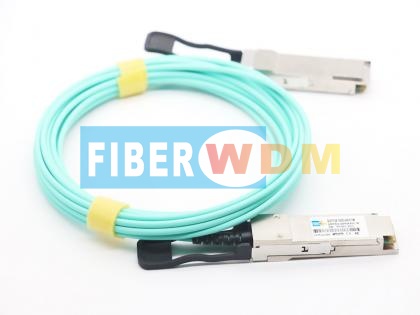
 1.6T OSFP-XD 2*FR4
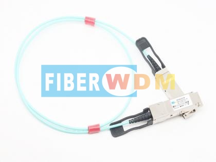
 1.6T OSFP-XD DR8+
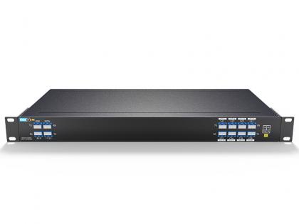
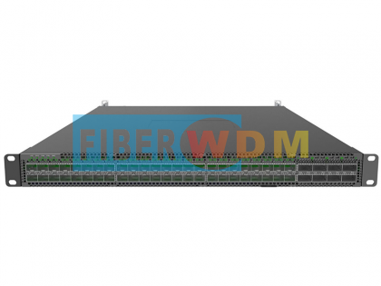 Data Center Switch 48x100Ge DSFP ports and 8x400Ge QSFP-DD uplink ports DS610
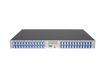 Idle Fiber Resource Management System
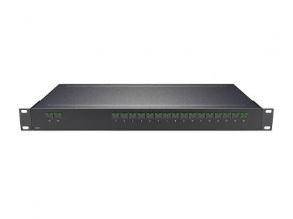 Splitter PLC 2X16 SC/APC 1U Rack 440*200*44mm
 100G CFP2 LR4 Dual Rate 10km Module
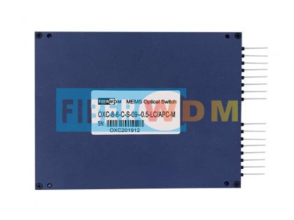 MXN MEMS Optical Switch
 Dual Fiber 18CH CWDM MUX DEMUX With Monitor Port

Address : Room 901, Building 6, JD Smart Industrial Park, No. 128, Juhua Stone Avenue, Huashan Town, Huadu District, Guangzhou City
Tel : +86 15989256178
Whatsapp : +86 15914235380
Email : sales@fiberwdm.com