
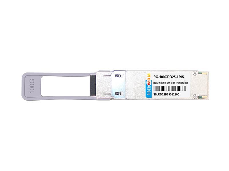
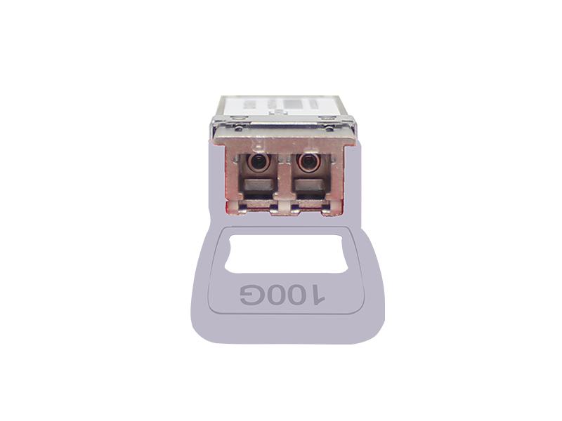
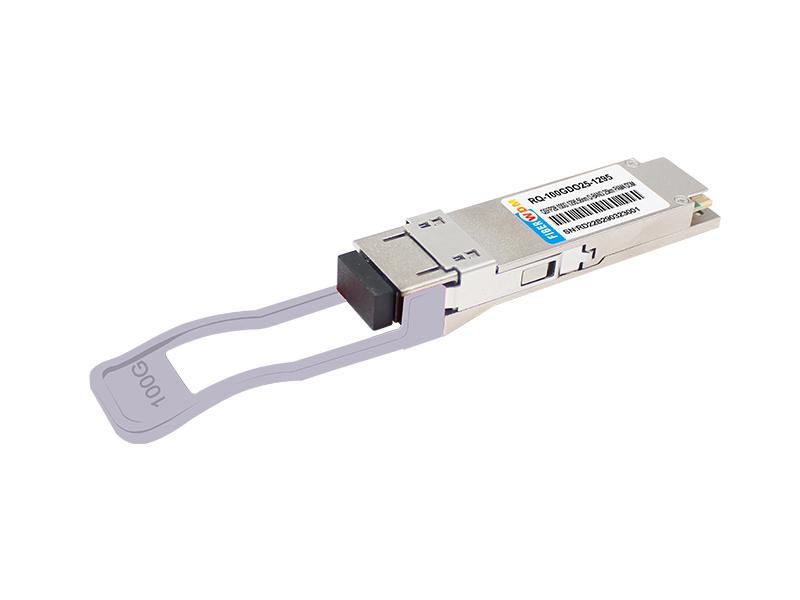
The RQ-100GDO25-XXXX series single mode transceiver module is designed for multiple channel 100GbE transmissions for up to 25km distance over standard G.652 single mode optical fiber (SMF) . The transceiver operates at a data rate of 100Gbps at the nominal DWDM wavelength from 1295.56nm to 1312.58nm as specified by the CW-WDM MSA. This module can convert 4 channels of 25Gbps (NRZ) electrical input data to 1 channel of 100Gbps (PAM4) optical signal, and also can convert 1 channel of 100Gbps (PAM4) optical signal to 4 channels of 25Gbps (NRZ) electrical output data. The electrical interface of the module is compliant with the OIF CEI-28G-VSR and QSFP28 MSA. It is designed to deploy in the RQ-100GDO25-XXXX SeriesQSFP28 100G O-Band DWDM 25KM SM LC Transceiver DWDM networking equipment in metropolitan access and core networks
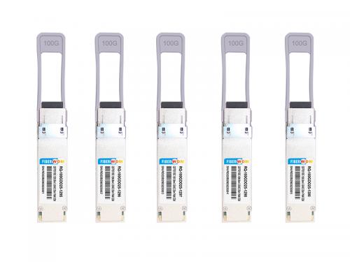
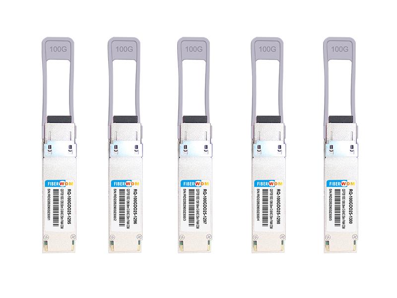
RQ-100GDO25-XXXX Series 100G QSFP28 O-Band DWDM 25KM SM LC Transceiver
Features
Applications
Ordering Information
| Part No. | Data Rate | Fiber | Distance*3 | Interface | Temp. |
| RQ-100GDO25-XXXX*2 | 100Gbps | SMF | 25km | LC | 0~+70°C |
*1: For the latest certification information, please check with FIBERWDM.
*2: XXXX refers to O-Band DWDM wavelength range as CW-WDM MSA specified, please refer the following table for detailed center wavelength information.
*3: Over G.652 SMF.
XXX-Channel refers to the following table
| Lane | Part NO. | Frequency (THz) | Center Wavelength (nm) |
| L-4 | RQ-100GDO25-1295 | 231.4 | 1295.56 |
| L-3 | RQ-100GDO25-1296 | 231.2 | 1296.68 |
| L-2 | RQ-100GDO25-1297 | 231.0 | 1297.80 |
| L-1 | RQ-100GDO25-1298 | 230.8 | 1298.93 |
| L0 | RQ-100GDO25-1300 | 230.6 | 1300.05 |
| L1 | RQ-100GDO25-1301 | 230.4 | 1301.18 |
| L2 | RQ-100GDO25-1302 | 230.2 | 1302.31 |
| L3 | RQ-100GDO25-1303 | 230.0 | 1303.45 |
| L4 | RQ-100GDO25-1304 | 229.8 | 1304.58 |
| L5 | RQ-100GDO25-1305 | 229.6 | 1305.72 |
| L6 | RQ-100GDO25-1306 | 229.4 | 1306.85 |
| L7 | RQ-100GDO25-1308 | 229.2 | 1308.00 |
| L8 | RQ-100GDO25-1309 | 229.0 | 1309.14 |
| L9 | RQ-100GDO25-1310 | 228.8 | 1310.28 |
| L10 | RQ-100GDO25-1311 | 228.6 | 1311.43 |
| L11 | RQ-100GDO25-1312 | 228.4 | 1312.58 |


Transmitter
As shown in Figure 1, the transmitter path of the transceiver contains a 4x25Gbps CAUI-4 electrical input, an integrated electrical multiplexer, a SiPho driver, a diagnostic monitor, a control and bias for the MZ modulator and a single mode laser source. The integrated electrical multiplexer converts 4 channels of 25Gbps (NRZ) electrical input data to 1 channel of 100Gbps (PAM4) optical signal.
Receiver
As shown in Figure 1, the receiver path of the transceiver contains an APD, a trans-impedance amplifier (TIA), an integrated de-multiplexer and a 4x25Gbps CAUI-4 compliant electrical output block. The integrated de-multiplexer converts 1 channel of 100Gbps (PAM4) optical signal to 4 channels of 25Gbps (NRZ) electrical output data.
High Speed Electrical Signal Interface
The interface between QSFP28 module and Host ASIC is shown in Figure 2. The high speed signal lines are internally AC-coupled and the electrical inputs are internally terminated to 100 Ohms differential. All transmitter and receiver electrical channels are compliant to CAUI-4 specification per IEEE 802.3cd.
Control Signal Interface
The module has the following low speed signals for control and status: ModSelL, ResetL, LPMode/TxDis, ModPrsL, IntL/RxLOSL. In addition, there is an industry standard two wire serial interface scaled for 3.3V LVTTL. The definition of control signal interface and the registers of the serial interface memory are further defined in the Control Interface& Memory Map section.
Handling and Cleaning
Exposure to current surges and overvoltage events can cause immediate damage to the transceiver module. Observe the precautions for normal operation of electrostatic discharge sensitive equipment, and attention should also be taken to restrict exposure to the conditions defined in the absolute maximum ratings.
Optical connectors will be exposed as long as the port plug is not inserted, so always pay attention to protection. Each module is equipped with a port guard plug to protect the optical ports. The protective plug shall always be in place whenever the optical fiber is not inserted. Before inserting the optical fiber, it is recommended to clean the end of the optical fiber connector to avoid contamination of the module optical port due to dirty connector. If contamination occurs, use standard LC port cleaning methods.
Absolute Maximum Ratings
Exceeding the absolute maximum ratings table may cause permanent damage to the device. This is just an emphasized rating, and does not involve the functional operation of the device that exceeds the specifications of this technical specification under these or other conditions. Long-term operation under absolute maximum ratings will affect the reliability of the device.
| Parameter | Symbol | Min. | Max. | Unit |
| Storage temperature | Ts | -40 | +85 | ℃ |
| Supply voltage | Vcc | -0.5 | 3.6 | V |
| Damage threshold | Rxdmg | -2.4 | dBm |
Recommended Operating Conditions*4
For operations beyond the recommended operating conditions, optical and electrical characteristics are not defined, reliability is not implied, and such operations for a long time may damage the module.
| Parameter | Symbol | Min. | Typical | Max. | Unit |
| Operating case temperature *5 | Tc | 0 | 70 | ℃ | |
| Power supply voltage | Vcc | 3.135 | 3.3 | 3.465 | V |
| Operating relative humidity | RH | 5 | 85 | % | |
| Power dissipation | PD | 5.5 | W | ||
| Electrical signal rate | 25.78125 | Gbps | |||
| Optical signal rate | 56.25 | Gbaud | |||
| Power supply noise*6 | 66 | mVpp | |||
| Receiver differential data output load | 100 | Ohm | |||
| Fiber length (9μm SMF) | 25 | km |
*4: Power supply specifications, instantaneous, sustained and steady state current are compliant with QSFP28 MSA power classification.
*5: The position of case temperature measurement is shown in Figure 9.
*6: Power supply noise is defined as the peak-to-peak noise amplitude over the frequency range at the host supply side of the recommended power supply filter with the module and recommended filter in place. Voltage levels including peak-to-peak noise are limited to the recommended operating range of the associated power supply. See Figure 7 for recommended power supply filter.
General Electrical Characteristics
Unless otherwise stated, the following characteristics are defined under recommended operating conditions.
| Parameter | Min. | Typical | Max. | Unit |
| Transceiver power consumption | 5.5 | W | ||
| Transceiver power supply current, Total | 1587 | mA | ||
| AC coupling capacitors (Internal) | 0.1 | μF |
Reference Points
| Reference point | Reference point |
| TP0 | Host ASIC transmitter output at ASIC package contact. |
| TP1 |
Input to module compliance board through mated module compliance board and module connector. Used to test module input. |
| TP1a |
Host ASIC transmitter output through the host board and host card edge connector at the output of the host compliance board. Also used to calibrate module input compliance signals. |
| TP4 |
Module output through the compliance board connectors at the output of the module compliance board. Also used to calibrate host input compliance signals. |
| TP4a | Input to host compliance board. Used to test host input. |
| TP5 | Input to host ASIC. |
| TP5a | Far end module output through a reference channel. |
Note: Individual standards may specify unique reference points.


High Speed Electrical Input Characteristics
Unless otherwise stated, the following characteristics are defined under recommended operating conditions.
| Parameter | Test Point | Min. | Typical | Max. | Unit | Conditions |
| Transmitter | ||||||
| Differential peak-peak input voltage tolerance | TP1a | 900 | mVp-p | |||
| Differential input impedance | TP1 | 90 | 100 | 110 | Ohm | |
| Output rise/fall time | TP1a | 10 | ps | 20%~80% | ||
| Eye width | TP1a | 0.46 | 1E-15 | |||
| Eye height , differential | TP1a | 95 | mV | 1E-15 | ||
| DC common mode voltage (Vcm)*7 | TP1 | -350 | 2850 | mV | ||
High Speed Electrical Output Characteristics
Unless otherwise stated, the following characteristics are defined under recommended operating conditions.
| Parameter | Test Point | Min. | Typical | Max. | Unit | Conditions |
| Differential peak-peak output voltage | TP4 | 900 | mVp-p | |||
| Differential output impedance | TP4 | 90 | 100 | 110 | Ohm | |
| Output rise/fall time | TP4 | 12 | ps | 20%~80% | ||
| Eye width | TP4 | 0.57 | UI | 1E-15 | ||
| Eye height differential | TP4 | 228 | mV | 1E-15 | ||
| DC common mode voltage (Vcm)*7 | TP4 | -350 | 2850 | mV |
*7: Vcm is generated by the host. Specification includes effects of ground offset voltage.
QSFP28 Transceiver Electrical Pad Layout

Package Outline
The module is designed to meet the package outline defined in the QSFP28 MSA specification. See the package outline for details.

Figure 8: Mechanical Package Outline (All dimensions in mm)
*This 2D drawing is only for reference, please check with FIBERWDM before ordering.
The bellow picture shows the location of the hottest spot for measuring module case temperature. In addition, the digital diagnostic monitors (DDM) temperature is also calibrated to this spot.

Control Interface Electrical Specifications
| Parameter | Symbol | Min. | Max. | Unit |
| SCL and SDA | VOL | 0 | 0.4 | V |
| VOH | VCC-0.5 | VCC+0.3 | V | |
| SCL and SDA | VIL | -0.3 | VCC*0.3 | V |
| VIH | VCC*0.7 | VCC+0.5 | V | |
| Capacitance on SCL and SDA I/O contact | Ci | - | 14 | pF |
| Total bus capacitive load for SCL and SDA | Cb | - | 100 | pF |
| - | 200 | pF | ||
| LPMode/TxDis, ResetL and ModSelL | VIL | -0.3 | 0.8 | V |
| VIH | 2 | Vcc+0.3 | V | |
| Iin | -365 | 125 | μA | |
| ModPrsL and IntL/RxLOSL | VOL | 0 | 0.4 | V |
| VOH | Vcc-0.5 | Vcc+0.3 | V |
Want to know about this product?
If you are interested in our products and want to know more details,please leave a message here,we will reply you as soon as we can.
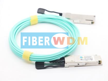
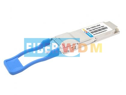
 100G QSFP28 SR4 100m 850nm MPO Optical Transceiver
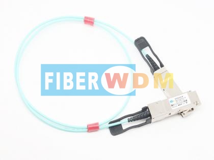
 100G QSFP28 CWDM4 10km LC Optical Transceiver
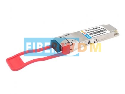
 100G QSFP28 LR4 1310nm 10km LC Optical Transceiver
 100G QSFP28 ER4 40Km 1310nm LC Optical Transceiver
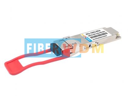
 100Gb QSFP28 ZR4 80Km 1310nm LC Optical Transceiver
 100G LR1 10km SFP-DD Optical Transceiver
 100G DWDM QSFP28 Dual CS Connector PAM4 Transceiver
 100GBASE-SR Bi-Directional QSFP28 850/900nm 100m DOM LC MMF Optical Transceiver Module

Address : Room 901, Building 6, JD Smart Industrial Park, No. 128, Juhua Stone Avenue, Huashan Town, Huadu District, Guangzhou City
Tel : +86 15989256178
Whatsapp : +86 15914235380
Email : sales@fiberwdm.com