
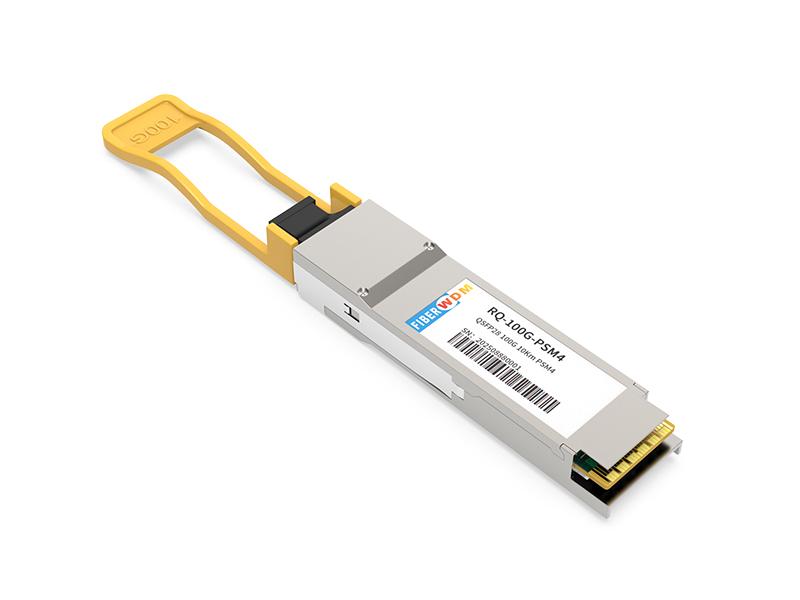
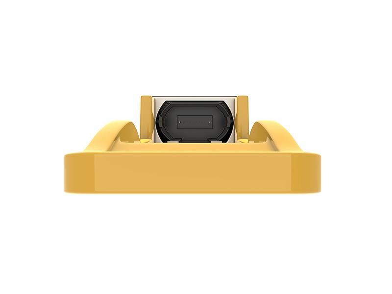
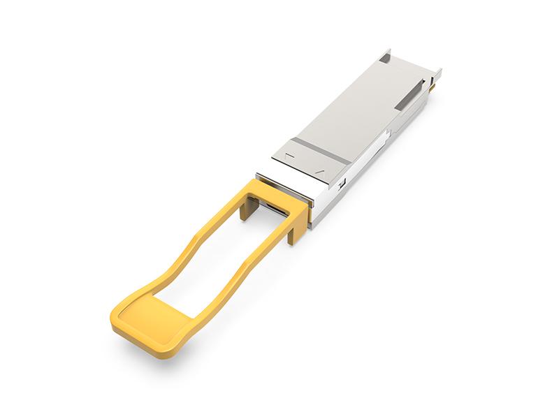
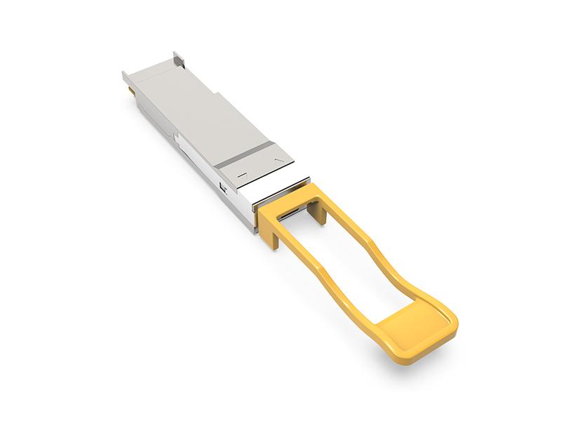
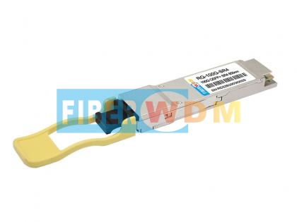
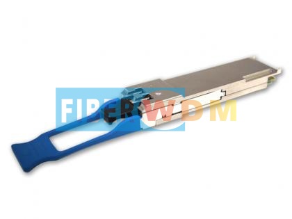
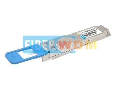
The RQ-100G-PSM4 QSFP28 optical transceiver is intended for up to 10km reach service with four-lane 25.78125G data rate. It is based on 3.3V DC power supply and operates in the commercial temperature range. It is compliant with QSFP MSA 、SFF-8436 、SFF-8636 and PSM4 MSA. Digital diagnostic functions are available via I2C interface,and the control functions can be achieved by LVTTL interfaces on the host,mainly including Module Select(ModSelL)、Module Reset(ResetL)、 Low Power Mode(LPMode). The transceiver incorporates a four-laser array which is usually DFB 、four-PIN diode array 、a high performance CDR integrated four drivers and TIAs IC separately. The differential AC coupled Tx and Rx data interfaces are CML compatible.
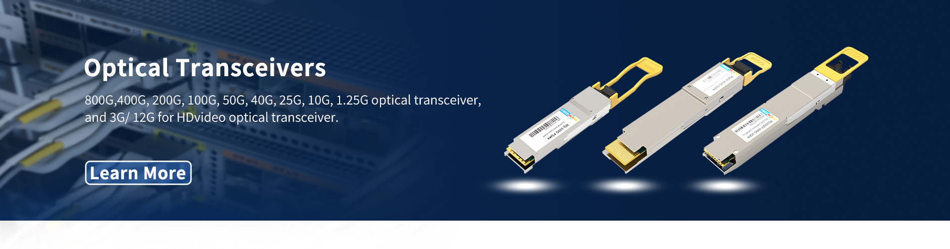
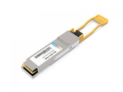
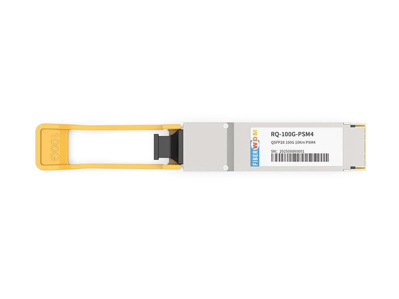
100G QSFP28 10km PSM4 Transceivers
Absolute maximum parameters
|
Absolute Maximum Ratings (EXCEEDING THESE RATINGS MAY CAUSE IRREVERSIBLE DAMAGE TO THE DEVICE) |
|||||
|
Parameter |
Symbol |
Min |
Max |
Units |
Notes |
|
Storage Temperature |
Tstg |
-40 |
+95 |
ºC |
Exceeding the absolute maximum ratings may cause irreversible damage to the device. The device is not intended to be operated under the condition of simultaneous absolute maximum rat- ings, which may cause irreversible damage to the device. |
|
Case Operating Temperature (Commercial ) |
TO |
0 | +70 |
ºC |
|
|
Relative Humidity - Storage |
RHS |
0 | 95 | % | |
|
Relative Humidity - Operating |
RHO |
0 | 85 | % | |
|
Supply Voltage |
VCC |
-0.3 | 3.6 | V | |
Operating conditions
|
Recommended Operating Conditions |
|||||
|
Parameter |
Symbol |
Min |
Typ |
Max |
Units |
|
Case Operating Temperature |
Tcase |
0 |
+70 |
ºC |
|
|
DC Supply Voltage |
VCC |
3.135 |
3.465 |
V |
|
|
Module Supply Current |
IIN |
1000 | mA | ||
Electrical Characteristics
|
Transmitter Electrical Characteristics |
|||||
|
Parameter |
Symbol |
Min |
Typ |
Max |
Units |
|
Differential Data input Swing |
VIN |
180 |
900 |
mV |
|
|
Tx Differential Input Impendence |
Zin |
90 | 100 | 110 |
Ω |
|
Tx Differential Output Impendence |
Zout |
45 | 50 | 55 |
Ω |
|
ResetL Disable Voltage |
Vr |
2.0 |
Vcc+0.3 |
V |
|
|
ResetL Enable Voltage |
VrEN |
0 |
0.8 |
V |
|
|
ModSelL Disable Voltage |
Vm |
2.0 |
Vcc+0.3 |
V |
|
|
ModSelL Enable Voltage |
VmEN |
0 |
0.8 |
V |
|
|
Receiver Electrical Characteristics |
|||||
|
Parameter |
Symbol |
Min |
Typ |
Max |
Units |
|
Differential Data Output Swing |
VOUT |
180 | 900 |
mV |
|
|
Rx Differential Output Impendence |
ZOUT |
90 | 100 | 110 |
Ω |
|
IntL Assert Voltage |
VInt |
VCC-0.5 |
VCC+0.3 |
V | |
|
IntL De-assert Voltage |
VDInt |
0 |
+0.4 |
V | |
Optical Specification
|
Transmitter Optical Specification |
||||||
|
Parameter |
Symbol |
Min |
Typ |
Max |
Units |
Notes |
|
Signal Rate|Each Lane |
25.78125±100ppm |
Gbps |
||||
|
Lane Wavelength |
L0 |
1295 |
1310 |
1325 |
nm |
|
|
L1 |
1295 |
1310 |
1325 |
nm |
||
|
L2 |
1295 |
1310 |
1325 |
nm |
||
|
L3 |
1295 |
1310 |
1325 |
nm |
||
|
Side Mode Suppression Ratio |
SMSR |
30 |
dB |
|||
|
Total Average Launch Power |
Ptol |
|
8.0 |
dBm |
||
|
Average Launch Power|Each Lane |
Pavg |
-9.4 | 2.0 |
dBm |
||
|
Optical Modulation Amplitude|Each Lane |
OMA |
2.2 |
dBm |
1 | ||
|
Transmitter and dispersion penalty|Each Lane |
TDP |
2.9 |
dB |
|||
|
Eye Mask coordinates: X1, X2, X3, Y1, Y2, Y3 |
|
{0.31, 0.4, 0.45, 0.34, 0.38, 0.4} |
|
2 | ||
|
Average launch power of OFF transmitter|Each Lane |
|
-30 |
dBm |
|||
|
Extinction Ratio |
ER |
3.5 |
dB |
|||
|
Spectral Width|20dB |
|
1 |
nm |
|||
|
Transmitter Reflectance |
|
-12 |
dB |
|||
|
Optical return loss tolerance |
|
20 |
dB |
|||
Note:
|
Receiver Optical Specification |
||||||
|
Parameter |
Symbol |
Min |
Typ |
Max |
Units |
Notes |
|
Signal Speed Per Lane |
25.78125±100ppm |
Gbps |
||||
|
Lane Wavelength |
L0 |
1295 |
1310 |
1325 |
nm |
|
|
L1 |
1295 |
1310 |
1325 |
nm |
||
|
L2 |
1295 |
1310 |
1325 |
nm |
||
|
L3 |
1295 |
1310 |
1325 |
nm |
||
|
Damage threshold|Each Lane |
THd |
3.0 |
dBm |
1 | ||
|
Average Receive Power|Each Lane |
-12.66 |
2.0 |
dBm |
|||
|
Receiver reflectance |
-26 |
dB |
||||
|
Sensitivity OMA|Each Lane[1] |
Sen |
-12.5 |
dBm |
2 | ||
|
Stressed Receiver Sensitivity (OMA), each Lane |
-8.8 |
dBm |
||||
|
LOS Assert |
LOSA |
-15.5 |
||||
|
LOS Deassert |
LOSD |
-13.5 |
||||
|
LOS Hysteresis |
LOSH |
0.5 | 3 | |||
|
Vertical Eye Closure Penalty |
VECP |
1.9 |
dB |
3 | ||
|
Stressed Eye J2 Jitter |
J2 |
0.27 |
UI |
|||
|
Stressed Eye J4 Jitter |
J4 |
0.39 |
UI |
|||
Note:
1. The receiver shall be able to tolerate, without damage, continuous exposure to a modulated optical input signal having this power level on one lane. The receiver does not have to operate correctly at this input power.
2. Measured with conformance test signal at receiver input for BER = 5e-5 BER.
3. Vertical eye closure penalty and stressed eye jitter are test conditions for measuring stressed receiver sensitivity. They are not characteristics of the receiver
Digital diagnosti
|
Monitoring Interface |
||||
|
Parameter |
Symbol |
Spec |
Units |
Condition/Notes |
|
Temperature |
Te |
+/-3 |
°C |
|
|
Voltage |
VCC |
+/-5% |
V |
|
|
IBias |
BIAS |
+/-10% |
mA |
|
|
Rx power |
Rx-pwr |
+/-2 |
dBm |
|
|
Tx power |
Tx-pwr |
+/-2 |
dBm |
|
Memery Map

PIN Assignmen

ModSelL
The ModSelL is an input pin. When held low by the host, the module responds to 2-wire serial communication commands. The ModSelL allows the use of multiple QSFP modules on a single 2-wire interface bus. When the ModSelL is “High”, the module shall not respond to or acknowledge any 2-wire interface communication from the host. ModSelL signal input node must be biased to the “High” state in the module.In order to avoid conflicts, the host system shall not attempt 2-wire interface communications within the ModSelL de-assert time after any QSFP modules are deselected. Similarly, the host must wait at least for the period of the ModSelL assert time before communicating with the newly selected module. The assertion and de-asserting periods of different modules may overlap as long as the above timing requirements are met
ResetL
The ResetL pin must be pulled to Vcc in the QSFP module. A low level on the ResetL pin for longer than the minimum pulse length (t_Reset_init) initiates a complete module reset, returning all user module settings to their default state. Module Reset Assert Time (t_init) starts on the rising edge after the low level on the ResetL pin is released. During the execution of a reset (t_init) the host shall disregard all status bits until the module inidicates a completion of the reset interrupt. The module indicates this by posting an IntL signal with the Data_Not_Ready bit negated. Note that on power up (including hot insertion) the module should post this completion of reset interrupt without requiring a reset.
ModPrsL
ModPrsL is pulled up to Vcc_Host on the host board and grounded in the module. The ModPrsL is asserted “Low” when inserted and deasserted “High” when the module is physically absent from the host connector
IntL
IntL is an output pin. When “Low”, it indicates a possible module operational fault or a status critical to the host system. The host identifies the source of the interrupt using the 2-wire serial interface.The IntL pin is an open collector output and must be pulled to host supply voltage on the host board.
LPMode
The LPMode pin shall be pulled up to Vcc in the QSFP module. This function is affected by the LPMode pin and the combination of the Power_over-ride and Power_set software control bits (Address A0h, byte 93 bits 0,1). The module has two modes a low power mode and a high power mode. The high power mode operates in one of the four power classes.When the module is in a low power mode it has a maximum power consumption of 1.5W. This protects hosts that are not capable of cooling higher power modules, should such modules be accidentally inserted.
The modules 2-wire serial interface and all laser safety functions must be fully operational in this low power mode. The module shall still support the completion of reset interrupt in this low power mode. If the Extended Identifier bits (Page 00h, byte 129 bits 6-7) indicate a power consumption greater than 1.5W and the module is in low power mode it must reduce its power consumption to less than 1.5W while still maintaining the functionality above. The exact method of accomplishing low power is not specified, however it is likely that either the Tx or Rx or both will not be operational in this state. If the Extended Identifier bits (Page 00h, byte 129 bits 6-7) indicate that its power consumption is less than 1.5W then the module shall be fully functional independent of whether it is in low power or high power mode.
The Module should be in low power mode if the LPMode pin is in the high state, or if the Power_ over-ride bit is in the high state and the Power_set bit is also high. The module should be in high power mode if the LPMode pin is in the low state, or the Power_over-ride bit is high and the Power_set bit is low. Note that the default state for the Power_over-ride bit is low.
Electrical Interface

Recommended PCB Layout


Mechanical Dimensions

Notes:
1、Tolerance: +/-0.1mm.
2、Others according to SFF-8661 or customer spec .
3、Optical port according to fiber connector spec.
Handling Precautions:
This device is susceptible to damage as a result of electrostatic discharge (ESD). A static free environment is highly recommended. Follow guidelines according to proper ESD procedures.
Laser Safety:
Radiation emitted by laser devices can be dangerous to human eyes. Avoid eye exposure to direct or indirect radiation.
Notice:
The information provided on this page contains the product target specifications which are subject to change without notice.
Check with your Litecore Sales Office for product updates, changes in specifications, sample availability and production release dates.
Want to know about this product?
If you are interested in our products and want to know more details,please leave a message here,we will reply you as soon as we can.
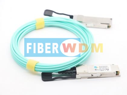
 100G QSFP28 SR4 100m 850nm MPO Optical Transceiver
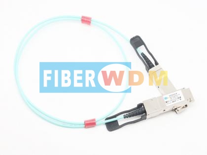
 100G QSFP28 CWDM4 10km LC Optical Transceiver
 100G QSFP28 LR4 1310nm 10km LC Optical Transceiver
 100G QSFP28 ER4 40Km 1310nm LC Optical Transceiver
 100Gb QSFP28 ZR4 80Km 1310nm LC Optical Transceiver
 100G LR1 10km SFP-DD Optical Transceiver
 100G DWDM QSFP28 Dual CS Connector PAM4 Transceiver
 100GBASE-SR Bi-Directional QSFP28 850/900nm 100m DOM LC MMF Optical Transceiver Module

Address : Room 901, Building 6, JD Smart Industrial Park, No. 128, Juhua Stone Avenue, Huashan Town, Huadu District, Guangzhou City
Tel : +86 15989256178
Whatsapp : +86 15914235380
Email : sales@fiberwdm.com