
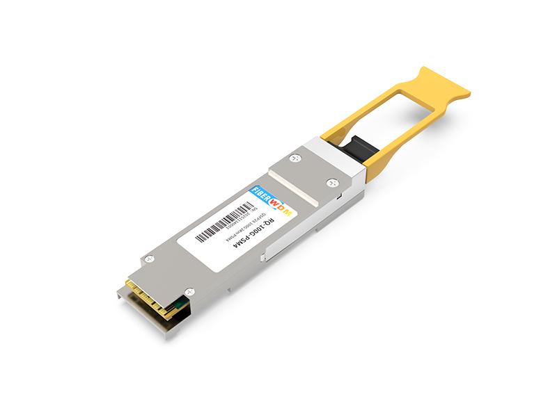
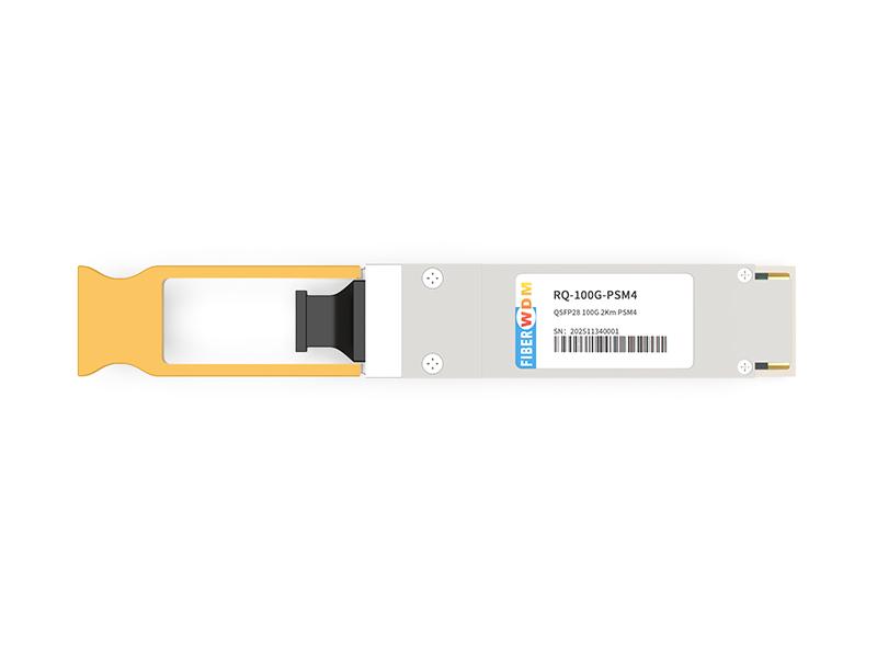
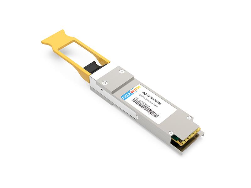
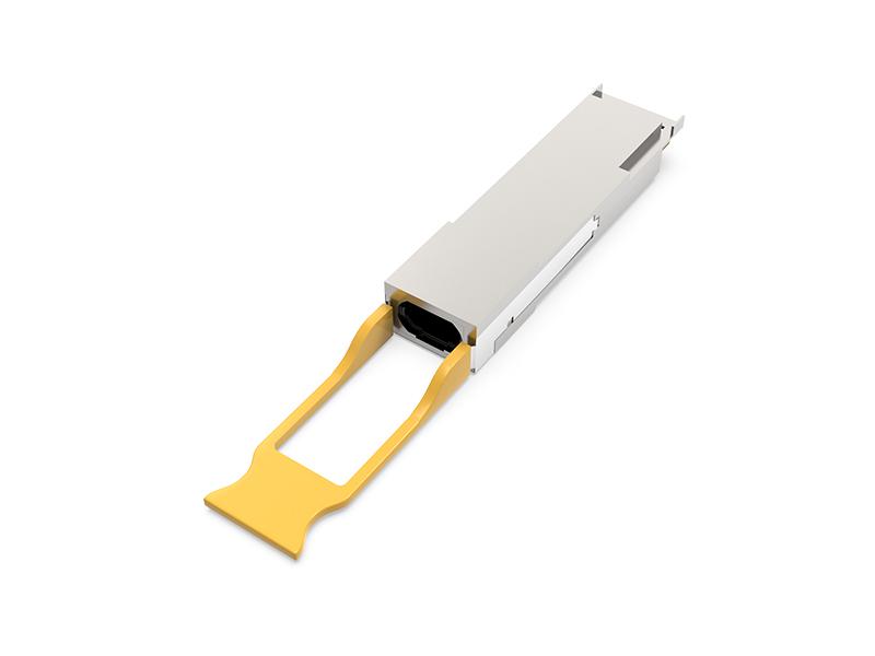
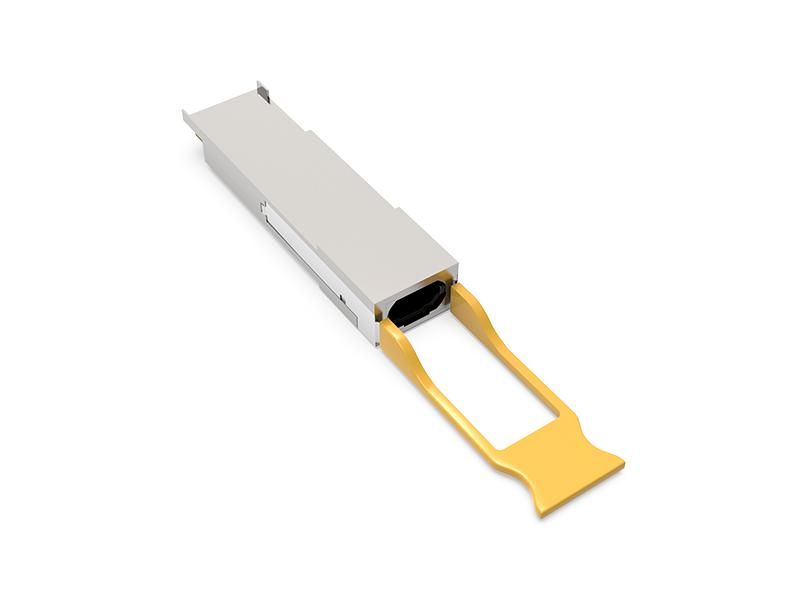
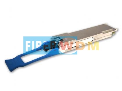
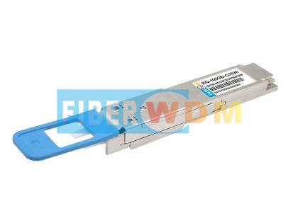
The QSFP28 PSM4 is a Four-Channel, Pluggable, Parallel, Fiber-Optic QSFP28 Transceiver for 100G Ethernet Applications. The QSFP28 full-duplex optical module offers 4 independent transmit and receive channels, each capable of 26Gbps operation for an aggregate data rate of 104Gbps 2km using single mode fiber. These modules are designed to operate over single mode fiber systems using DFB laser array. An optical fiber ribbon cable with an MPO/MTPTM connector can be plugged into the QSFP28 module receptacle. QSFP28 PSM4 is one kind of parallel transceiver which provides increased port density and total system cost savings.
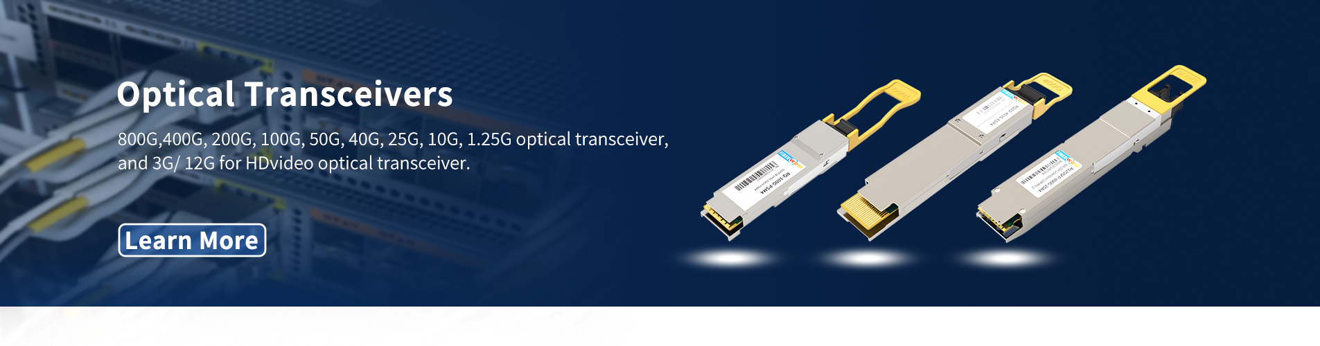
100Gb/s QSFP28 PSM4 2km Optical Transceiver
Product Features
Applications
Ordering Information
|
Feature |
Standard |
Performance |
|
Electromagnetic Interference (EMI) |
FCC Part 15 Class B EN 55022:2010, Class B |
Compatible with standards |
|
Electromagnetic susceptibility (EMS) |
EN 55024:2010 |
Compatible with standards |
|
Laser Eye Safety |
FDA 21CFR 1040.10 and 1040.11 EN60950, EN (IEC) 60825-1,2 |
Compatible with Class laser product |
Absolute Maximum Ratings
The operation in excess of any absolute maximum ratings might cause permanent damage to this module.
|
Parameter |
Symbol |
Min |
Max |
Unit |
|
Storage Temperature |
TS |
-40 |
85 |
degC |
|
Operating Case Temperature |
TOP |
0 | 70 |
degC |
|
Power Supply Voltage |
VCC |
-0.3 |
3.6 | V |
|
Relative Humidity (non-condensation) |
RH |
0 | 85 |
% |
|
Input Voltage |
Vin |
-0.3 |
Vcc+0.3 |
V |
Recommended Operating Conditions and Power Supply Requirements
|
Parameter |
Symbol |
Min |
Typical |
Max |
Unit |
Notes |
|
Operating Case Temperature |
TOP |
0 | 70 |
degC |
Operating Case Temperature |
|
|
Power Supply Voltage |
VCC |
3.135 |
3.3 |
3.465 |
V |
Power Supply Voltage |
|
Power Consumption |
3.5 | W |
Power Supply Voltage |
|||
|
Data Rate |
DR |
25.78125 |
Gbps |
Data Rate |
||
|
Data Speed Tolerance |
∆DR |
-100 |
+100 |
ppm |
Data Speed Tolerance |
|
|
Link Distance with G.652 |
D | 0 | 2 | km |
Link Distance with G.652 |
Electrical Characteristics
|
Parameter |
Test Point |
Min |
Typical |
Max |
Unit |
|
Differential input impedance |
Zin |
90 | 100 | 110 |
ohm |
|
Differential Output impedance |
Zout |
90 | 100 | 110 |
ohm |
|
Differential input voltage amplitude |
ΔVin |
300 | 1100 |
mVp-p |
|
|
Differential output voltage amplitude |
ΔVout |
300 | 800 |
mVp-p |
|
|
Input Logic Level High |
VIH |
2.0 | VCC |
V |
|
|
Input Logic Level Low |
VIL |
0 | 0.8 |
V |
|
|
Output Logic Level High |
VOH |
VCC-0.5 |
VCC |
V |
|
|
Output Logic Level Low |
VOL | 0 | 0.4 |
V |
Optical Characteristics
|
Parameter |
Symbol |
Min |
Typical |
Max |
Unit |
Notes |
|
Transmitter |
||||||
|
Center Wavelength |
λC |
1295 | 1325 |
nm |
1 | |
|
RMS Spectral Width |
λrms |
3.5 |
nm |
1 | ||
|
Average Launch Power, each lane |
PAVG |
-6 | -0.5 |
+2.0 |
dBm |
|
|
Optical Modulation Amplitude (OMA) |
POMA |
-5 | -0.5 |
+2.2 |
dBm |
1 |
|
Difference in Launch Power between any two lanes |
Ptx,diff |
5.0 |
dB |
|||
|
Transmitter and dispersion penalty (TDP), each lane (max) |
TDP |
2.9 |
dBm |
1 | ||
|
Rise/Fall Time |
Tr/Tf |
30 | ps | |||
|
Extinction Ratio |
ER |
3.5 |
dB |
|||
|
Relative Intensity Noise |
Rin |
-128 |
dB/Hz |
|||
|
Optical Return Loss Tolerance |
TOL |
20 |
dB |
|||
|
Transmitter Reflectance |
RT |
-12 |
dB |
|||
|
Transmitter Eye Mask Margin |
EMM |
10 |
% |
2 | ||
|
Average Launch Power OFF Transmitter, each Lane |
Poff |
|
-30 |
dBm |
||
|
Transmitter Eye Mask Definition {X1, X2, X3, Y1, Y2, Y3} |
{0.31,0.4,0.45, 0.34,0.38,0.4} |
|||||
|
Receiver |
||||||
|
Center Wavelength |
λC |
1295 |
1325 | nm | ||
|
Damage Threshold |
THd |
+3 |
dBm |
|||
|
Overload, each lane |
OVL |
+2.5 |
dBm |
|||
|
Receiver Sensitivity in OMA, each Lane |
SEN |
-11.35 |
dBm |
3 | ||
|
Signal Loss Assert Threshold |
LOSA |
-30 |
dBm |
|||
|
Signal Loss Deassert Threshold |
LOSD |
-12 |
dBm |
|||
|
LOS Hysteresis |
LOSH |
0.5 |
dB |
|||
|
Optical Return Loss |
ORL |
-12 |
dBm |
|||
Notes:
1. Transmitter wavelength, RMS spectral width and power need to meet the OMA minus TDP specs to guarantee link performance.
2. The eye diagram is tested with 1000 waveform.
3. Measured with a PRBS 231 -1 test pattern, @25.78Gb/s, BER<5*10 -5
Digital Diagnostic Functions
The following digital diagnostic characteristics are defined over the normal operating conditions unless otherwise specified.
|
Parameter |
Symbol |
Min | Max | Unit | Notes |
|
Temperature monitor absolute error |
DMI_Temp |
-3 |
3 |
degC |
Over operating temp |
|
Supply voltage monitor absolute error |
DMI _VCC |
-0.1 |
0.1 |
V |
Full operating range |
|
Channel RX power monitor absolute error |
DMI_RX |
-3 |
3 |
dB |
Per channel |
|
Channel Bias current monitor |
DMI_Ibias |
-10% |
10% |
mA |
Per channel |
|
Temperature monitor absolute error |
DMI_Temp |
-3 | 3 |
degC |
Over operating temp |
Power Supply Filtering
The host board should use the power supply filtering shown in Figure1.

Figure1. Host Board Power Supply Filtering
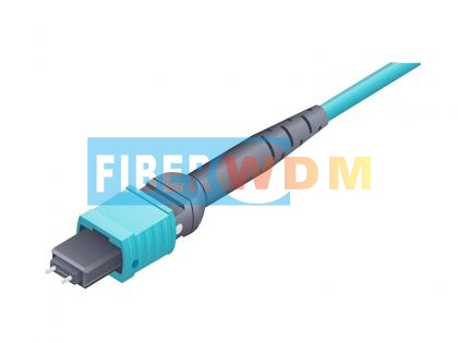
Optical Interface Lanes and Assignment
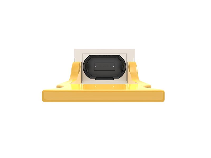
The optical interface port is a male MPO connector. The four fiber positions on the left as shown in Figure 2, with the key up, are used for the optical transmit signals (Channel 1 through4). The fiber positions on the right are used for the optical receive signals (Channel 4 through 1). The central four fibers are physically present.

Figure 2. Optical Receptacle and Channel Orientation
Mechanical Dimensions

Attention: To minimize MPO connection induced reflections, an MPO receptacle with 8-degree angled end-face is utilized for this product. A male MPO connector with 8-degree end-face should be used with this product as illustrated in Figure 5.

ESD
This transceiver is specified as ESD threshold 1kV for SFI pins and 2kV for all other electrical input pins, tested per MIL-STD-883, Method 3015.4 /JESD22-A114-A (HBM). However, normal ESD precautions are still required during the handling of this module. This transceiver is shipped in ESD protective packaging. It should be removed from the packaging and handled only in an ESD protected environment.
Laser Safety
This is a Class 1 Laser Product according to IEC 60825-1:2007. This product complies with 21 CFR 1040.10 and 1040.11 except for deviations pursuant to Laser Notice No. 50, dated (June 24, 2007).
Pin Assignment and Description

Pin Assignment
|
PIN # |
Logic |
Symbol |
Description |
| 1 |
GND |
Ground |
|
| 2 |
CML-I |
Tx2n |
Transmitter Inverted Data Input |
| 3 |
CML-I |
Tx2p |
Transmitter Non-Inverted Data output |
| 4 |
GND |
Ground |
|
| 5 |
CML-I |
Tx4n |
Transmitter Inverted Data Input |
| 6 |
CML-I |
Tx4p |
Transmitter Non-Inverted Data output |
| 7 |
GND |
Ground |
|
| 8 |
LVTLL-I |
ModSelL |
Module Select |
| 9 | LVTLL-I |
ResetL |
Module Reset |
| 10 |
VccRx |
+3.3V Power Supply Receiver |
|
| 11 |
LVCMOS-I/O |
SCL |
2-Wire Serial Interface Clock |
| 12 |
LVCMOS-I/O |
SDA |
2-Wire Serial Interface Data |
| 13 |
GND |
Ground |
|
| 14 |
CML-O |
Rx3p |
Receiver Non-Inverted Data Output |
| 15 |
CML-O |
Rx3n |
Receiver Inverted Data Output |
| 16 |
GND |
Ground |
|
| 17 |
CML-O |
Rx1p |
Receiver Non-Inverted Data Output |
| 18 |
CML-O |
Rx1n |
Receiver Inverted Data Output |
| 19 |
GND |
Ground |
|
| 20 |
GND |
Ground |
|
| 21 |
CML-O |
Rx2n |
Receiver Inverted Data Output |
| 22 |
CML-O |
Rx2p |
Receiver Non-Inverted Data Output |
| 23 |
GND |
Ground |
|
| 24 |
CML-O |
Rx4n |
Receiver Inverted Data Output |
| 25 |
CML-O |
Rx4p |
Receiver Non-Inverted Data Output |
| 26 |
GND |
Ground |
|
| 27 |
LVTTL-O |
ModPrsL |
Module Present |
| 28 |
LVTTL-O |
IntL |
Interrupt |
| 29 |
VccTx |
+3.3 V Power Supply transmitter |
|
| 30 |
Vcc1 |
+3.3 V Power Supply |
|
| 31 |
LVTTL-I |
LPMode |
Low Power Mode |
| 32 |
GND |
Ground |
|
| 33 |
CML-I |
Tx3p |
Transmitter Non-Inverted Data Input |
| 34 |
CML-I |
Tx3n |
Transmitter Inverted Data Output |
| 35 |
GND |
Ground |
|
| 36 |
CML-I |
Tx1p |
Transmitter Non-Inverted Data Input |
| 37 |
CML-I |
Tx1n |
Transmitter Inverted Data Output |
| 38 |
GND |
Ground |
Want to know about this product?
If you are interested in our products and want to know more details,please leave a message here,we will reply you as soon as we can.
 100G QSFP28 SR4 100m 850nm MPO Optical Transceiver
 100G QSFP28 CWDM4 10km LC Optical Transceiver
 100G QSFP28 LR4 1310nm 10km LC Optical Transceiver
 100G QSFP28 ER4 40Km 1310nm LC Optical Transceiver
 100Gb QSFP28 ZR4 80Km 1310nm LC Optical Transceiver
 100G LR1 10km SFP-DD Optical Transceiver
 100G DWDM QSFP28 Dual CS Connector PAM4 Transceiver
 100GBASE-SR Bi-Directional QSFP28 850/900nm 100m DOM LC MMF Optical Transceiver Module

Address : Room 901, Building 6, JD Smart Industrial Park, No. 128, Juhua Stone Avenue, Huashan Town, Huadu District, Guangzhou City
Tel : +86 15989256178
Whatsapp : +86 15914235380
Email : sales@fiberwdm.com