
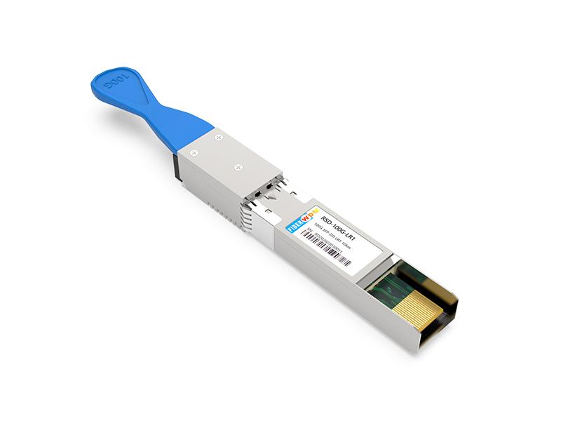
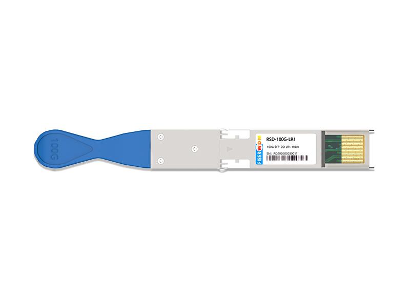
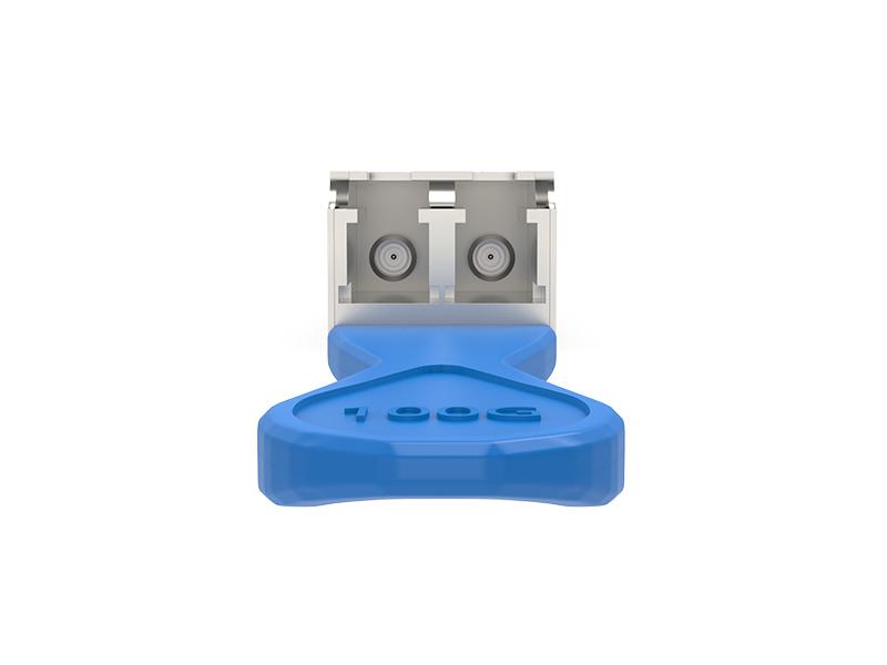
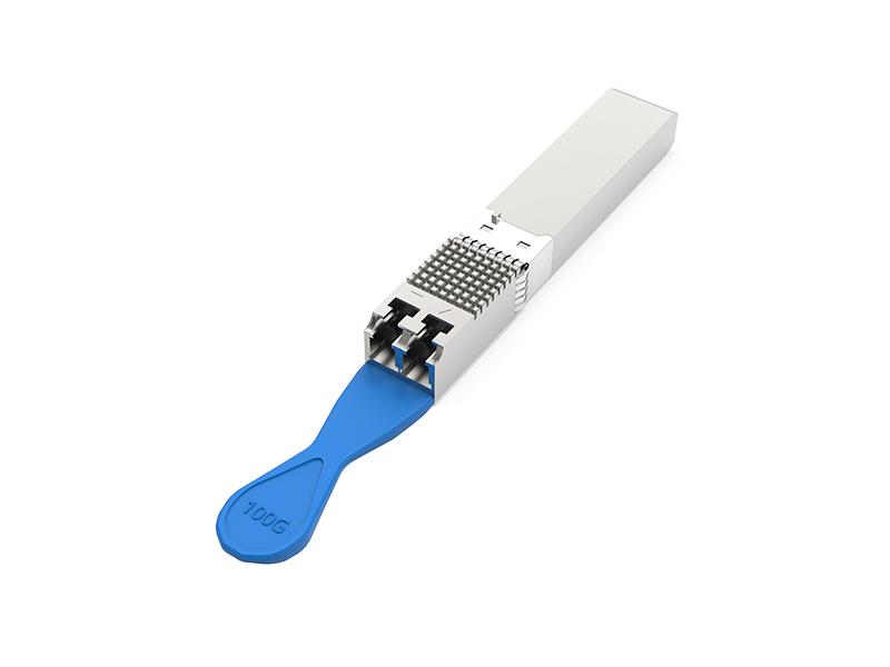
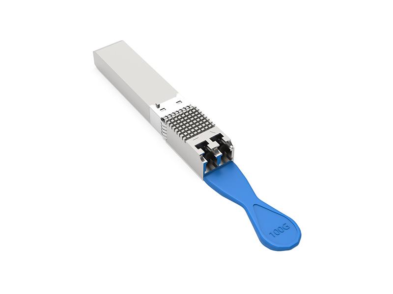
The 100G LR1 SFP56-DD optical transceiver, 100G SFP56-DD LR1 is designed for using in 100-Gigabit Ethernet links up to 10km over Single-Mode Fiber (SMF). It is compliant with the SFP56-DD MSA,IEEE802.3CU,100G Lambda 100G LR1 and 100GAUI-2(no FEC)1. Digital diagnostics functions are available via the I2C interface, as specified by the SFP56-DD MSA.
The module incorporates 1 channel optical signal, on 1311nm center wavelength, operating at 100Gbps data rate. This module can convert 2 channels of 53Gbps (PAM4) electrical input data to 1 channel of 106Gbps (PAM4) optical signal, and also can convert 1 channel of 106Gbps (PAM4) optical signal to 2 channels of 53Gbps (PAM) electrical output data. The optical interface uses a Duplex LC connector. The high performance cooled EML transmitter and high sensitivity PIN receiver provide superior performance for 100Gigabit Ethernet applications up to 10km links.
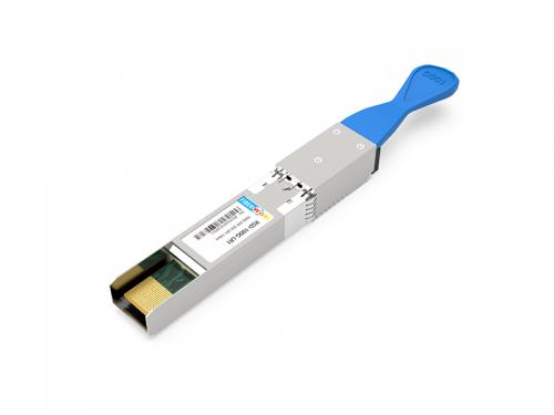
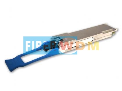
100G LR1 10km SFP-DD Optical Transceiver RSD-100G-LR1
Features
Applications
Note:
1. KR-FEC is optional, please contact us if necessary.

Figure 1. Module Block Diagram
Absolute Maximum Ratings
| Parameter | Symbol | Min | Max | Unit |
| Supply Voltage | Vcc | -0.3 | V | |
| Input Voltage | Vin | -0.3 | Vcc+0.3 | V |
| Storage Temperature | Ts | -20 | 85 | ºC |
| Case Operating Temperature | Tc | 0 | 70 | ºC |
| Humidity (non-condensing) | Rh | 5 | 85 | % |
Recommended Operating Conditions
| Parameter | Symbol | Min | Typical | Max | Unit |
| Supply Voltage | Vcc | 3.13 | 3.3 | 3.47 | V |
| Operating Case temperature | Tc | 0 | 70 | ºC | |
| Data Rate Per Lane | fd | 106.25 | Gb/s | ||
| Humidity | Rh | 5 | 85 | % | |
| Power Dissipation | Pm | 3 | 3.5 | W | |
| Link Distance with G.652 | D | 10 | km |
Electrical Specifications
| Parameter | Symbol | Min | Typical | Max | Unit |
| Differential Input Impedance | Zin | 90 | 100 | 110 | ohm |
| Differential Output Impedance | Zout | 90 | 100 | 110 | ohm |
| Differential Input Voltage Amplitude1 | ΔVin | 1600 | mVp-p | ||
| Differential Output Voltage Amplitude2 | ΔVout | 900 | mVp-p |
Note:
1. Differential input voltage amplitude is measured between TxnP and TxnN.
2. Differential output voltage amplitude is measured between RxnP and RxnN.
Optical Characteristics
| Parameter | Symbol | Min | Typical | Max | Unit | Notes |
| Transmitter | ||||||
| Centre Wavelength | λc | 1304.5 | 1317.5 | nm | ||
| Side-mode suppression ratio | SMSR | 30 | dB | |||
| Average launch power | Pout | -1.4 | 4.5 | dBm | ||
| Transmitter and dispersion eye closure(TDECQ) | TDECQ | 3.4 | dB | |||
| Extinction Ratio | ER | 3.5 | dB | |||
| Average launch power of OFF transmitter | -30 | dB | ||||
| Receiver | ||||||
| Centre Wavelength | λc | 1304.5 | 1317.5 | nm | ||
| Receiver Sensitivity in OMA outer | RXsen | -6.1 | dBm | 1 | ||
| Average receive power | Pin | -7.7 | 4.5 | dBm | ||
| Receiver Reflectance | -26 | dB | ||||
| LOS Assert | -13 | dBm | ||||
| LOS De-Assert – OMA | -11 | dBm | ||||
| LOS Hysteresis | 0.5 | dB | ||||
Pin Description


Note:
1. SFP-DD uses common ground (GND) for all signals and supply (power). All are common within the SFP-DD module and all module voltages are referenced to this potential unless otherwise noted. Connect these directly to the host board signalcommon ground plane.
2. VccR, VccT shall be applied concurrently and VccR1, VccT1 shall be applied concurrently. Requirements defined for the host side of the Host.The connector Vcc pins are each rated for a maximum current of 1000 mA.
3. The ePPS pins (if not used) may be terminated with 50 to ground on the host.

Figure 2. Electrical Pin-out Details
Speed1, Speed2, Speed1DD, Speed2DD
Speed1, Speed2, Speed1DD and Speed2DD are module inputs and are pulled low to GND with >30 k resistors in the module. Speed1 optionally selects the optical receive signaling rate for channel 1. Speed1DD optionally selects the optical receive signaling rate for channel 2. Speed2 optionally selects the optical transmit signaling rate for the channel 1. Speed2DD optionally selects the optical transmit signaling rate for channel 2.
Note: At 128 GFC the FC LSN no longer require to use Speed1, Speed2, Speed1DD and Speed2DD, it is under consideration to reclaim these signals for programmable or other functions.
ResetL Pin
Reset. LPMode_Reset has an internal pull-up in the module. A low level on the ResetL pin for longer than the minimum pulse length (t_Reset_init) initiates a complete module reset, returning all user module settings to their default state. Module Reset Assert Time (t_init) starts on the rising edge after the low level on the ResetL pin is released. During the execution of a reset (t_init) the host shall disregard all status bits until the module indicates a completion of the reset interrupt. The module indicates this by posting an IntL signal with the Data_Not_Ready bit negated. Note that on power up (including hot insertion) the module will post this completion of reset interrupt without requiring a reset.
Mod_ABS
Mod_ABS must be pulled up to Vcc Host on the host board and pulled low in the module. The Mod_ABS is asserted “Low” when the module is inserted. The Mod_ABS is deasserted “High” when the module is physically absent from the host connector due to the pull up resistor on the host board.
LPMode
LPMode is an input signal from the host operating with active high logic. The LPMode signal must be pulled up to Vcc in the SFP-DD/SFP-DD112 module. The LPMode signal allows the host to define whether the SFP- DD/SFP-DD112 module will remain in Low Power Mode until software enables the transition to High Power Mode as defined in the SFP-DD management specification. In Low Power Mode (LPMode de-asserted Low), the module may immediately transition to High Power Mode after the management interface is initialized.
ResetL
The ResetL signal shall be pulled to Vcc in the module. A low level on the ResetL signal for longer than the minimum pulse length (t_Reset_init) initiates a complete module reset, returning all user module settings to their default state.
Power Supply Filtering
The host board should use the power supply filtering shown in Figure 3.

Figure 3. Host Board Power Supply Filtering
DIAGNOSTIC MONITORING INTERFACE (OPTIONAL)
The following digital diagnostic characteristics are defined over the normal operating conditions unless otherwise specified.
| Parameter | Symbol | Min | Max | Units | Notes |
| Temperature monitor absolute error | DMI_Temp | -3 | +3 | degC | Over operating temperature range |
| Supply voltage monitor absolute error | DMI _VCC | -0.1 | 0.1 | V | Over full operating range |
| Channel RX power monitor absolute error | DMI_RX_Ch | -2 | 2 | dB | 1 |
| Channel Bias current monitor | DMI_Ibias_Ch | -10% | 10% | mA | |
| Channel TX power monitor absolute error | DMI_TX_Ch | -2 | 2 | dB | 1 |
Notes:
1. Due to measurement accuracy of different single mode fibers, there could be an additional +/-1 dB fluctuation, or a +/- 3 dB total accuracy.
Digital diagnostics functions are available via the I2C interface as specified by SFP-DD MIS. The SFP-DD MIS management memory is shown in Figure 4.
Due to eight-bit addresses, This limits the management memory that can be directly accessed by the host to 256 bytes, which is divided in Lower Memory (addresses 00h through 7Fh) and Upper Memory (addresses 80h through FFh).
The addressing structure of the additional internal management memory1 is shown in Figure 5. The
management memory inside the module is arranged as a unique and always host accessible address space of 128 bytes (Lower Memory) and as multiple upper address subspaces of 128 bytes each (Pages), only one of which is selected as host visible in Upper Memory. A second level of Page selection is possible for Pages for which several instances exist (e.g. where a bank of pages with the same Page number exists).
This structure supports a flat 256 byte memory for passive copper modules and permits timely access to addresses in the Lower Memory, e.g. Flags and Monitors. Less time critical entries, e.g. serial ID information and threshold settings, are available with the Page Select function in the Lower Page. For more complex modules which require a larger amount of management memory the host needs to use dynamic mapping of the various Pages into the host addressable Upper Memory address space, whenever needed.
Note: The management memory map has been designed largely after the CMIS memory map where pages and banks are used in order to enable time critical interactions between host and module while expanding the memory size. This memory map has been changed in order to accommodate just two electrical lanes and to limit the required memory. The single address approach is used as found in QSFP.

Figure 4. QSFP28 Memory Map

Figure 5. SFP-DD MIS Bank Page Memory Map

Figure 6. The Lower Memory Overview

Figure 7. Page 00h Memory Overview

Figure 8. Page 01h Memory Overview

Figure 9. Page 13h Memory Overview

Figure 10. Page 14h Memory Overview
Mechanical Dimensions

Figure 11. Mechanical Specifications
References
1. SFP-DD MSA
2. IEEE802.3cu 100GBASE-LR1
3. 100G Lambda MSA 100G LR1-10
Ordering Information
| Part Number | Product Description |
| RSD-100G-LR1 | SFP56-DD LR1, 106.25Gb/s, 10km, EML+PIN, SMF, Dual LC |
Want to know about this product?
If you are interested in our products and want to know more details,please leave a message here,we will reply you as soon as we can.
 100G QSFP28 SR4 100m 850nm MPO Optical Transceiver
 100G QSFP28 CWDM4 10km LC Optical Transceiver
 100G QSFP28 LR4 1310nm 10km LC Optical Transceiver
 100G QSFP28 ER4 40Km 1310nm LC Optical Transceiver
 100Gb QSFP28 ZR4 80Km 1310nm LC Optical Transceiver
 100G DWDM QSFP28 Dual CS Connector PAM4 Transceiver
 100GBASE-SR Bi-Directional QSFP28 850/900nm 100m DOM LC MMF Optical Transceiver Module
 100GBASE-LR Bi-Directional QSFP28 1280/1310nm 20km LC SM Optical Transceiver Module

Address : Room 901, Building 6, JD Smart Industrial Park, No. 128, Juhua Stone Avenue, Huashan Town, Huadu District, Guangzhou City
Tel : +86 15989256178
Whatsapp : +86 15914235380
Email : sales@fiberwdm.com