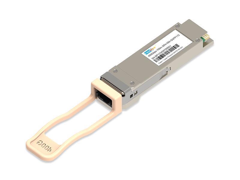
The 400G QSFP112 SR4 Transceiver is designed to transmit and receive serial optical data links up to 106.25 Gb/s data rate (per channel) by PAM4 modulation format over multi-mode fiber. It is a small-form- factor hot pluggable transceiver module integrated Optical Extinction Ratio 2.5 dB with high performance vcsel. It is compliant with 400G Ethernet specs and QSFP112 MSA.
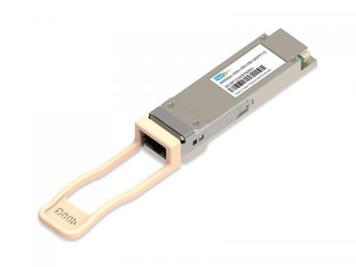
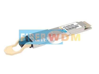
QSFP112 400G BASE-SR4 850nm 100m Transceiver
Application
Features
Specification
| Parameter | Symbol | Unit | Min | Typ | Max | Notes |
| Transmitter (Per Lane) | ||||||
| Signaling Speed Per Lane | GBd | 53.125±100pm | ||||
| Modulation Format | PAM4 | |||||
| Center Wavelength | nm | 844 | 850 | 863 | ||
| RMS Spectral Width | RMS | dB | 0.6 | |||
| Average Launch Power Per Lane | TXPx | dBm | -4.6 | 4 | ||
| Outer Optical Modulation Amplitude Per Lane | OMAouter | dBm | -2.6 | 3.5 | ||
| Transmitter Excursion, Each Lane | DPx | dB | 2.3 | |||
|
Transmitter and Dispersion Penalty Eye Closure for PAM4, Each Lane |
TDECQ | dB | 4.4 | |||
|
Average Launch Power of Off Transmitter, Each Lane |
dBm | -30 | ||||
| Transmitter Transition Time | Tr、Tf | ps | 17 | |||
| Optical Extinction Ratio | ER | dB | 2.5 | |||
| RIN12OMA | dB/Hz | -132 | ||||
| Optical Return Loss Tolerance | dB | 12 | ||||
| Encircled Flux | ≥86% at 19mm, ≤30% at 4.5 mm | |||||
| Parameter | Symbol | Unit | Min | Typ | Max | Notes |
| Receiver (Per Lane) | ||||||
| Signaling Speed Per Lane | GBd | 53.125±100pm | ||||
| Modulation Format | PAM4 | |||||
| Input Operating Wavelength | nm | 842 | 948 | |||
| Damage Threshold Per Lane | DT | dBm | 5 | |||
| Average Receive Power Per Lane | RXPx | dBm | -6.4 | 4 | ||
| Receive Power OMAouter Per Lane | OMAouter | dBm | 3.5 | |||
| Receiver Reflectance | Rfl | -12 | ||||
|
Receiver Sensitivity (OMAouter),Each Lane |
dBm | -4.6 | ||||
| Stressed Sensitivity (OMAouter) | 5 | dBm | -2 |
BER=2.4E-4 TDECQ=4.4 |
||
Ordering Information
| Part No | Specifications | Application | ||||||||
| Package | Data rate | Laser | Optical Power | Detector | Sensitivity | Temp | Reach | Others | ||
|
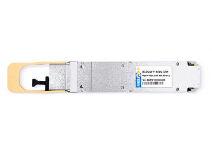
RQ112-400G-SR4 |
QSFP112 | 400G | VCSEL | -4.6~4dBm | PIN | <-4.6dBm@OMA | 0~70 ℃ | 100M | RoHS |
400G Base SR4 |
Absolute Maximum Ratings
| Parameter | Symbol | Unit | Min | Max |
| Storage Temperature Range | Ts | ℃ | -40 | +85 |
| Relative Humidity | RH | % | 5 | 95 |
| Power Supply Voltage | Vcc | V | -0.5 | +4.0 |
Recommended Operating Conditions
| Parameter | Symbol | Unit | Min | Typ | Max |
| Operating Case Temperature Range | Tc | ℃ | 0 | / | 70 |
| Power Supply Voltage | Vcc | V | 3.135 | 3.3 | 3.465 |
Optical Interface
 Figure 1 Optical Lane Sequence
Principle Diagram
 Figure 2 Module Principle Diagram
Electric Ports Definition
| Parameter | Symbol | Unit | Min | Typ | Max | Notes |
| Supply Voltage | VCC | V | 3.14 | 3.47 | ||
| Supply Current | ICC | mA | 3000 | |||
| Transceiver Power-on Initialize Time | mS | 2000 | ||||
| Transmitter | ||||||
| PAM4 Signaling Rate Per Lane | BR | GBd | 53.125 | PAM4 | ||
| Single Ended Input Voltage Tolerance | VinT | V | -0.3 | 4.0 | ||
| Differential Data Input Swing | VIN | mVp-p | 880 | |||
| Common Mode Noise (RMS) | mV | 17.5 | ||||
|
Differential Differential Termination Resistance Mismatch |
% | 10 | ||||
|
Receiver |
||||||
|
PAM4 Signaling Rate Per Lane |
GBd | 53.125 | ||||
|
Single Ended Output Voltage |
VoutR | V | 0.45 | |||
|
Differential Data Output Swing |
Vout,PP | mVp-p | 900 | |||
|
Common Mode Noise (RMS) |
mV | 17.5 | ||||
|
Differential Differential Termination Resistance Mismatch |
% | 10 | ||||
|
IIC communication |
||||||
|
IIC Clock Frequency (Fast Mode) |
MHZ | 1 | ||||
|
Clock Stretching |
us | 500 | ||||
|
Data Hold Time |
ns | 300 | ||||

Figure 3 Electrical Pin-out Details
Pin Descriptions
| Pin No | Logic | Symbol | Description | Note |
| 1 | GND | Ground | 1 | |
| 2 | CML-I | Tx2n | Transmitter Inverted Data Input | |
| 3 | CML-I | Tx2p | Transmitter Non-Inverted Data output | |
| 4 | GND | Ground | 1 | |
| 5 | CML-I | Tx4n | Transmitter Inverted Data Input | |
| 6 | CML-I | Tx4p | Transmitter Non-Inverted Data output | |
| 7 | GND | Ground | 1 | |
| 8 | LVTTL-I | ModSelL | Select | |
| 9 | LVTTL-I | ResetL | Reset | |
| 10 | VccRx | +3.3V Power Supply Receiver | 2 | |
| 11 | LVCOMS-I/O | SCL | 2-Wire Serial Interface Clock | |
| 12 | LVCOMS-I/O | SDA | 2-Wire Serial Interface Data | |
| 13 | GND | Ground | 1 | |
| 14 | CML-0 | Rx3p | Receiver Non-Inverted Data Output | |
| 15 | CML-0 | Rx3n | Receiver Inverted Data Output | |
| 16 | GND | Ground | 1 | |
| 17 | CML-0 | Rx1p | Receiver Non-Inverted Data Output | |
| 18 | CML-0 | Rx1n | Receiver Inverted Data Output | |
| 19 | GND | Ground | 1 | |
| 20 | GND | Ground | 1 | |
| 21 | CML-0 | Rx2n | Receiver Inverted Data Output | |
| 22 | CML-0 | Rx2p | Receiver Non-Inverted Data Output | |
| 23 | GND | Ground | 1 | |
| 24 | CML-0 | Rx4n | Receiver Inverted Data Output | |
| 25 | CML-0 | Rx4p | Receiver Non-Inverted Data Output | |
| 26 | GND | Ground | 1 | |
| 27 | LVTTL-0 | ModPrsL | Present | |
| 28 | LVTTL-0 | IntL/RxLOS | Interrupt/optional RxLOS | |
| 29 | VccTx | +3.3 V Power Supply transmitter | 2 | |
| 30 | Vcc1 | +3.3 V Power Supply | 2 | |
| 31 | LVTTL-I | LPMode/TxDis | Low Power Mode/optional TX Disable | |
| 32 | GND | Ground | 1 | |
| 33 | CML-I | Tx3p | Transmitter Inverted Data Input | |
| 34 | CML-I | Tx3n | Transmitter Non-Inverted Data output | |
| 35 | GND | Ground | 1 | |
| 36 | CML-I | Tx1p | Transmitter Inverted Data Input | |
| 37 | CML-I | Tx1n | Transmitter Non-Inverted Data output | |
| 38 | GND | Ground | 1 | |
| 39 | GND | Ground | 1 | |
| 40 | CML-I | Tx6n | Transmitter Inverted Data Input | |
| 41 | CML-I | Tx6p | Transmitter Non-Inverted Data output | |
| 42 | GND | Ground | 1 | |
| 43 | CML-I | Tx8n | Transmitter Inverted Data Input | |
| 44 | CML-I | Tx8p | Transmitter Non-Inverted Data output | |
| 45 | GND | Ground | 1 | |
| 46 | Reserved | For future use | 3 | |
| 47 | VS1 | Module Vendor Specific 1 | 3 | |
| 48 | VccRx1 | +3.3V Power Supply Receiver | 2 | |
| 49 | VS2 | Module Vendor Specific 2 | 3 | |
| 50 | VS3 | Module Vendor Specific 3 | 3 | |
| 51 | GND | Ground | 1 |
Notes:
1. GND is the symbol for signal and supply (power) common for the QSFP112 module. All are common within the QSFP112 module and all voltages are referenced to this potential unless otherwise noted. Connect these directly to the host board signal- common ground plane. 2. Vcc Rx, Vcc1 and Vcc Tx are the receiver and transmitter power supplies and shall be applied concurrently. Requirements, defined for the host side of the Host Edge Card Connector, are listed in Table 4. Recommended host board power supply filtering is shown in Figure 4. Vcc Rx, Vcc1and Vcc Tx may be internally connected within the QSFP112 module in any combination. The connector pins are each rated for a maximum current of 1.5A (max. current of 2.0 A is required for high module power of 15- 20W).
Module Memory Map


Figure 4 Digital Diagnostic Memory Map
Host Board Power Supply Filtering
Any voltage drop across a filter network on the host is counted against the host DC set point accuracy specification. Inductors with DC Resistance of less than 0.1 Ohm should be used in order to maintain the required voltage at the Host Edge Card Connector. Figure5 is the suggested transceiver/host interface.

Figure 5 Recommended Host Board Power Supply Filtering
Package Outline

Want to know about this product?
If you are interested in our products and want to know more details,please leave a message here,we will reply you as soon as we can.
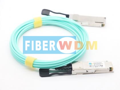
 400G QSFP-DD DR4 PAM4 1310nm 500M MPO Optical Transceiver
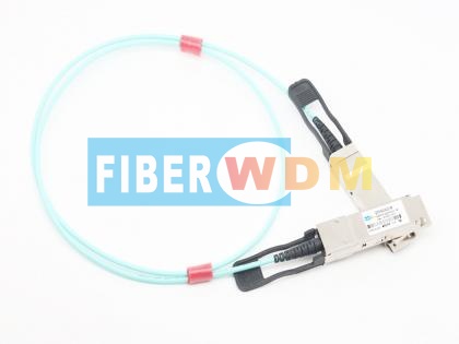
 400G QSFP-DD SR8 850nm MPO 100M Optical Transceiver
 400G QSFP-DD LR4 10KM Optical Transceiver
 400G CFP2 DCO Optical Transceiver Module
 400G OSFP SR4 MM MPO12 Optical Transceiver IB
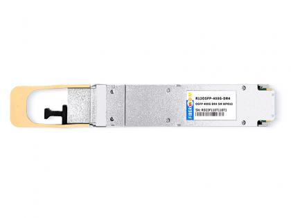 400G OSFP DR4 SM MPO12 Optical Transceiver IB
 400G QSFP-DD FR4 2KM Optical Transceiver
 400G QSFP-DD EDR4 SM MPO12 2km Optical Transceiver

Address : Room 901, Building 6, JD Smart Industrial Park, No. 128, Juhua Stone Avenue, Huashan Town, Huadu District, Guangzhou City
Tel : +86 15989256178
Whatsapp : +86 15914235380
Email : sales@fiberwdm.com